
Composition-Dependent Phonon and Thermodynamic Characteristics of C-Based XxY1−xC (X, Y ≡ Si, Ge, Sn) Alloys

1
Department of Physics, University of North Florida, 1 UNF Drive, Jacksonville, FL 32224-7699, USA
2
Department of Physics, Indiana University of Pennsylvania, 975 Oakland Avenue, 56 Weyandt Hall, Indiana, PA 15705-1087, USA
Inorganics 2024, 12(4), 100; https://doi.org/10.3390/inorganics12040100
Submission received: 28 February 2024
/
Revised: 26 March 2024
/
Accepted: 27 March 2024
/
Published: 30 March 2024
(This article belongs to the Special Issue Optical and Quantum Electronics: Physics and Materials)
Abstract
:Novel zinc-blende (zb) group-IV binary XC and ternary XxY1−xC alloys (X, Y ≡ Si, Ge, and Sn) have recently gained scientific and technological interest as promising alternatives to silicon for high-temperature, high-power optoelectronics, gas sensing and photovoltaic applications. Despite numerous efforts made to simulate the structural, electronic, and dynamical properties of binary materials, no vibrational and/or thermodynamic studies exist for the ternary alloys. By adopting a realistic rigid-ion-model (RIM), we have reported methodical calculations to comprehend the lattice dynamics and thermodynamic traits of both binary and ternary compounds. With appropriate interatomic force constants (IFCs) of XC at ambient pressure, the study of phonon dispersions offered positive values of acoustic modes in the entire Brillouin zone (BZ)—implying their structural stability. For XxY1−xC, we have used Green’s function (GF) theory in the virtual crystal approximation to calculate composition x, dependent and one phonon density of states . With no additional IFCs, the RIM GF approach has provided complete in the crystallographic directions for both optical and acoustical phonon branches. In quasi-harmonic approximation, the theory predicted thermodynamic characteristics (e.g., Debye temperature ΘD(T) and specific heat Cv(T)) for XxY1−xC alloys. Unlike SiC, the GeC, SnC and GexSn1−xC materials have exhibited weak IFCs with low [high] values of ΘD(T) [Cv(T)]. We feel that the latter materials may not be suitable as fuel-cladding layers in nuclear reactors and high-temperature applications. However, the XC and XxY1−xC can still be used to design multi-quantum well or superlattice-based micro-/nano devices for different strategic and civilian application needs.
1. Introduction
Since the invention of Si-based transistors [1], the evolution to include them in radio frequency (RF) devices for microelectronics has been remarkable [2,3,4,5,6,7,8,9,10,11]. With the low processing costs, Si-technology has led to many achievements by incorporating electrodes, dielectrics, and other elements in different integrated circuits (ICs). With truly monolithic optoelectronic functionality, Si has offered substantial cost benefits as well as long-term performance gains in the optoelectronic microsensor systems [12,13,14,15,16] and photovoltaic cells. These achievements have given tremendous opportunities for both the scientists and engineers to successfully incorporate different devices in energy harvesting and gas-sensing needs. Earlier accomplishments on RF devices and ICs have quickly grown to become valuable for wireless sensor networks (WSNs) [17,18]. These devices are now employed in a wide range of applications including photonics, optoelectronics, environment monitoring, medical diagnostics, forensic, spintronics, cellular base phone transceivers, amplifiers, Gigabit wireless local as well as personal area networks [12,13,14,15,16,17,18,19,20,21,22,23,24,25,26,27,28,29,30,31,32].
The progress in Si-based ICs and WSNs is the outcome of many scientific research reports published on different topics where materials’ perspectives played increasingly important roles. New wavelength regimes are now extended from 1.55 μm to 5.0 μm for the operations of Si-based photonic and opto-electronic ICs [10]. While many multiple-quantum-wells (MQWs) and superlattices (SLs) based III-V semiconductors [19,20,21,22] have revealed extremely inspiring results, the high cost and incompatibility of III-Vs with the Si platform has been, and still is, the main impediment that prevented the large-scale commercial production of different opto-electronic devices [23,24,25,26,27,28,29,30,31,32,33,34,35,36,37,38].
Despite the technological achievements of group-IV materials, the IV-IV binary XC and ternary XxY1−xC alloys with X, Y (≡Si, Ge, and Sn) have recently become quite attractive in preparing different heterostructures for bandgap and strain engineering [29,30,31,32]. At room temperature (RT), the C, Si, Ge, and α-Sn of diamond crystal structures are known to exhibit indirect band gap energies [≡5.47 eV, 1.12 eV, 0.66 eV and 0 eV]. Higher mismatch between the lattice constants, [≡C: 3.56 Å, Si: 5.43 Å, Ge: 5.66 Å, α-Sn: 6.49 Å] and low solubility of C has caused complications in the earlier designs of XC/Si MQWs and SLs [33,34,35,36,37,38,39,40,41,42,43,44,45]. However, the differences in their electronegativity now play a vital role in carefully optimizing parameters to achieve epitaxial growth of heterostructures apposite for diverse device applications. Recently, the use of Si/SiGe has gained considerable attention for designing heterojunction bipolar transistors with cut-off frequencies > 10 GHz [11].
Tremendous efforts have also been formulated in preparing novel C-based binary XC and/or ternary XxY1−xC alloys by taking advantage of the unique and exciting properties of group-IV materials [12,13,14,15,16,17,18,19,20,21,22,23,24,25,26,27,28,29,30,31,32,33,34,35,36,37]. Good structural stability of zinc-blende (zb) binary and/or ternary compounds with different , hardness, high stiffness, melting point, and high thermal conductivity is considered particularly favorable for applications [38,39,40,41] in blue/ultraviolet (UV) light-emitting diodes (LEDs), laser diodes (LDs), photodetectors and solar cells [12,13,14,15,16], etc. Due to large lattice mismatch and the differences in thermal expansion coefficients between XxY1−xC epilayers and Si substrate, one would expect the possibilities of observing structural and/or intrinsic defects near the interfaces [29]. However, appropriate use of buffer layers acquiring load through the relaxation of mechanical stresses has helped improve the structural qualities of MQWs and SLs. While there remain a few intrinsic issues, which could constrain the design of opto-electronic device structures, solutions to these problems are not impossible and can be resolved by exploiting suitable experimental (e.g., growth, [42,43,44,45,46,47,48,49,50,51,52,53,54,55,56,57,58,59,60,61,62,63,64,65,66,67,68,69,70,71,72,73,74,75,76,77,78,79,80,81,82,83,84,85,86,87,88,89,90,91,92,93] characterization [94,95,96,97,98,99,100,101,102,103,104,105,106,107]) and theoretical [108,109,110,111,112,113,114,115,116,117,118,119,120,121,122,123,124,125,126,127,128,129,130,131,132,133,134,135,136,137] methods.
One must note that by employing the pulsed supersonic free jets techniques [42,43,44,45], an inverse heteroepitaxial growth of Si on SiC has been demonstrated to achieve multilayer structures [46,47,48,49,50,51,52,53,54,55,56,57,58,59,60,61,62,63,64,65]. A novel arc plasma C gun source is incorporated in the molecular beam epitaxial (MBE) methods to grow ultrathin MQWs and SLs [66,67,68,69,70]. Ultrahigh chemical vapor deposition (UH-CVD), reduced pressure RP-CVD and metalorganic (MOCVD) techniques are also successfully used [71,72,73,74,75,76,77,78,79,80,81,82,83,84,85,86,87,88,89,90,91,92,93] to prepare different Si1−xGexC/Si, Ge1−xSnxC/Si, GeC/SiC epilayers. For commercial applications of these materials, the RP-CVD method has been preferred due to the balance between good epitaxial quality and relatively high growth rates [76]. Certainly, the progress made in the growth of complex and exotic C-based materials has set challenges for both the physicists and engineers in investigating their fundamental properties.
Although binary compounds are used in many technological applications, considerably less attention is paid to ternary alloys despite the successful growth of ultrathin epifilms. A variety of characterization techniques are also applied for analyzing/ monitoring their fundamental properties [94,95,96,97,98,99,100,101,102,103,104,105,106,107]. The classification of such methods includes reflection high-energy electron diffraction (RHEED) [94,95], Auger electron spectroscopy (AES) [96], He+ Rutherford backscattering spectrometry (RBS) [97], atomic force microscopy (AFM) [98,99], high-resolution X-ray diffraction (HR-XRD) [100,101,102], transmission electron microscopy (XTEM) [103], photoluminescence (PL) [104], absorption, Fourier transform infrared (FTIR) spectroscopy [100,101,102], Raman scattering spectroscopy (RSS) [105,106,107] and spectroscopic ellipsometry (SE) techniques [107], etc. It is to be noted that not only have these techniques validated their crystal structures but also helped in assessing the film thickness, strain, intrinsic electrical, and optical traits. Despite the existence of numerous experimental studies on structural and electrical properties, there are limited IR absorption and RSS measurements [100,101,102,103,104,105,106,107] for evaluating their phonon characteristics.
From a theoretical standpoint, several calculations are performed to understand the structural, electronic, and optical properties of the binary compounds using full potential linear augmented plane wave (FP-LAPW), first-principles (ab initio) and molecular dynamical (MD) methods [108,109,110,111,112,113,114,115,116,117,118,119,120,121,122,123,124,125,126]. For the ternary XxY1−xC alloys, however, no systematic studies are known for comprehending their lattice dynamical and/or thermodynamic characteristics. To accomplish major technological applications of the C-based heterostructures [e.g., Si/Si(Ge)C, GeSnC/GeC MQWs and (SiC)m/(Ge(Sn)C)n SLs], such calculations are necessary to obtain the complete phonon dispersions of XC and XxY1−xC materials from realistic lattice dynamical models. One reason for this requisite is that the dynamical response of polar lattices affects the key electronic properties, including the exciton-binding energies and charge-carrier mobilities. Examining the dynamical response of crystals and its impact on the dielectric environment provides a major step in realizing their structural characteristics. The other reason for its need is that, in MQWs and SLs, the phonon density of states (DOS) of binary/ternary alloys has played crucial roles in evaluating thermodynamic traits, including the thermal expansion coefficients α(T), Debye temperature ΘD(T), heat capacity Cv(T), Grüneisen constants γ(T), entropy, lattice thermal conductivity, etc.
The purpose of this work is to use a realistic rigid-ion model (RIM) [127] and report the methodical results of our comprehensive study to assess the structural, lattice dynamical (cf. Section 2.1), and thermodynamic (cf. Section 2.2) characteristics of binary XC and ternary (cf. Section 2.3) X1−xYxC alloys. For the tetrahedral (: ) binary materials, we have carefully optimized the RIM interatomic force constants (IFCs) by exercising [128] (cf. Section 2.1.1) successive least-square fitting procedures. In these processes, the phonon frequencies at high critical points (Γ, X, and L) are used as input while exploiting their lattice—, and elastic constants as constraints (see Table 1). For zb-SiC, the values of phonon frequencies are incorporated from inelastic X-ray scattering (IXS) measurements [129], while in GeC, SnC, we employed critical-point phonon frequencies from first-principles ABINIT results using a plane–wave pseudopotential method in density functional theory (DFT) and local-density perturbation approximation [125]. With the appropriate IFCs of binary XC materials, the dynamical matrix (cf. Section 3 and Section 3.1) is diagonalized to obtain phonon dispersions at each wave vector point in the Brillouin zone (BZ), as well as one phonon density of states (DOS), . For mixed XxY1−xC alloys 0 ≤ x ≤ 1, the composition-dependent phonon frequencies (cf. Section 3.2) are simulated by using a Green’s function (GF) theory [130] in the virtual crystal approximation (VCA). Without considering additional IFCs, the RIM GF approach for the mixed alloys has offered a complete dependent in arbitrary crystallographic directions for both the optical and acoustical phonon branches. In XxY1−xC materials, and using a quasi-harmonic approximation (QHA), we have systematically simulated the x-dependent and (cf. Section 3.2) to predict their thermodynamic characteristics (e.g., Debye temperature ΘD(T) and specific heat Cv(T)). Born’s transverse effective charges , and Fröhlich coupling parameters are also (cf. Section 3.2.3 and Section 3.2.4) calculated. Theoretical results of , and the thermo-dynamical traits for both binary XC and ternary XxY1−xC alloys are carefully analyzed/contrasted (cf. Section 3.1) against the existing experimental [129] and theoretical [120,121,122,123,124,125,126] data (cf. Section 3) with concluding remarks presented in Section 4.
2. Computational Details
The vibrational properties of XC materials have played a valuable role in assessing their phase transitions, transport coefficients and other physical phenomena [130,131,132,133,134,135,136,137]. Understanding the electron–phonon interactions and polaron characteristics in polar compounds is important for evaluating their optical and transport properties [138]. In X1−xYxC alloys, the exploration of phonons and optical and structural characteristics is crucial for correlating them to their different microscopic traits. To the best of our knowledge, no experimental and/or theoretical studies of phonons exist for X1−xYxC alloys, especially ones examining the contributions of lattice dynamical properties to phonon-free energy, entropy, specific heat, and Debye temperatures, etc. Accurate RIM simulations of and for the binary XC materials are employed (cf. Section 2.1) to comprehend the lattice dynamics and thermodynamic properties of X1−xYxC alloys using a GF methodology (cf. Section 2.2).
2.1. Phonons in XC Materials
Earlier, the IXS [129] and RSS results [105] of phonon dispersions for the zb 3C-SiC were analyzed by exploiting the ab initio methods [120,121,122,123,124,125,126]. Recent calculations of lattice dynamics for GeC and SnC using plane–wave pseudopotential DFT approaches in the local density approximation [124,125] have provided different results. By using a realistic RIM [127], we have probed the experimental and theoretical data [105,120,121,122,123,124,125,126,129] of phonon dispersions for binary XC (3C-SiC, GeC and SnC) materials. Our choice of RIM, briefly described in Section 2.1.1, is based on the following facts: (a) a truncated RIM [139,140,141,142,143,144], where the number of IFCs is limited, a priori, failed to give accurate and it is not even less complicated than the more realistic scheme [127] adopted here; and (b) with regard to , our simulated results in the high-symmetry direction are comparable (cf. Section 3) with experimental (3C-SiC) [105,129] and ab initio methods (GeC, SnC) [120,121,122,123,124,125,126].
2.1.1. Rigid-Ion Model
Here, we have briefly outlined the RIM [127] to comprehend the vibrational and thermodynamic properties of perfect binary XC materials. In this approach, the atomic displacements of the jth vibrational modes , are expressed as plane waves with the wave vector as [127]:
where t is the time; the and are, respectively, the position and mass of the atom. The term represents the position and denotes the types of atoms with = 1, 2 to specify the C and X, respectively, in the XC materials (see: the crystal structure, in Figure 1a, and its BZ in Figure 1b).
In the harmonic approximation, the equations of motion can be expressed either in terms of the force constant matrix elements [127]:
or in terms of the dynamical matrix elements:
where,
The term [] in Equations (2a)–(2c) represents the force constant [dynamical] matrix elements involving components of both the short-range and long-range Coulomb interactions [127,139,140,141,142,145,146,147]. For simulating the of binary materials, the short- (A, B, Cκ, Dκ, Eκ and Fκ) and long-range (Zeff) interactions involved in and matrices are optimized (Table 2) following successive non-linear least-square fitting procedures.
In the primitive unit cell of the zb lattice having two atoms per unit cell, the solutions of Equations (2a) and (2b) lead to an eigenvalue problem of size (6 × 6) with the values of wave vectors restricted to the fcc lattice:
with the triplets distributed uniformly throughout the volume of the BZ. In our calculations of phonon dispersions for the XC materials, we have used a mesh of 64,000 || points in the reduced BZ. At each , there are six [127] vibrational modes—three of them are acoustic (i.e., a longitudinal and a doubly degenerate transverse ) and the remaining modes are optical, comprising a doubly degenerate transverse— and a longitudinal optical phonons (cf. Section 3.1).
2.2. Lattice Dynamics of Ternary XxY1−xC Alloys
Composition-dependent phonon dispersions for mixed zb XxY1−xC crystals are simulated as a function of x (0 ≤ x ≤ 1) (cf. Section 3.2) by adopting a generalized GF theory in the VCA. For one dimensional mixed XxY1−xC alloy with two interpenetrating sublattices, Kutty [131] has developed a GF approach and derived the dynamical matrix equation:
by postulating that the sublattice 1 occupies C atoms while the sublattice 2 is randomly acquired by atoms of type X and Y having concentrations (x) and (1 − x), respectively. In Equation (4), , , , , , and the term represents the IFCs. By substituting these parameters in Equation (4), we obtain the following [131]:
with the solution of Equation (5) leading to the vibrational mode frequencies.
Extension of the above one-dimensional approach to simulate the lattice dynamics of three-dimensional ideal zb random XxY1−xC ternary alloys using GF theory [131] in the framework of a RIM [127] is trivial. Here, we have assumed that the mixed XxY1−xC crystal lattice achieves the following: (a) forms the ideal pseudo-binary alloys in the entire composition range x, (probably in contrast to reality), (b) the cation sublattice 2 is structurally close to the virtual crystal lattice where the X and Y atoms are randomly distributed having the concentration of Y (1 − x) and of X as x, (c) the anion sublattice 1 with C atoms remains undistorted, and (d) the characteristic NN atomic distances follow Vegard’s law. It is to be noted that in the RIM GF methodology, no additional IFCs are required for the descriptions of wave-vector dependent phonon dispersions of the XxY1−xC alloys in arbitrary crystallographic directions. To simulate the dynamical characteristics of the pseudo-binary alloys using RIM, we have deliberated the IFCs of binary XC materials (cf. Table 2) in a three-body framework. While this approach has allowed for the calculations of phonon spectra for the optical, acoustical as well as disorder-induced modes, we have neglected here the disorder-related broadening of the spectral lines.
2.3. Thermodynamic Properties
To comprehend the effects of temperature on the structural stability of XC materials, we have calculated the thermodynamic properties (up to 1500 K) in the QHA by adopting a RIM and including appropriate values of their and [132,133,134,135,136,137,138]. In the numerical computation of T-dependent lattice heat capacity (), we have used the following:
where is the total static energy at 0 K which can be calculated by first-principles methods, is the zero-point vibrational energy, is Boltzmann’s constant, ħ is Planck’s constant. The term can be expressed as follows:
The lattice contribution to is obtained by using [138] the following:
From Debye’s equation,
it is possible to calculate . In Equation (9), the term r signifies the number of atoms per unit cell.
2.4. Interaction of Photons with Solids
In polar materials, the electrical polarization induced by the displacement of atoms offers the key quantities to understand how the deformations and electric fields are coupled, insulating them. The interaction of photons with solids comprises both ionic and electronic oscillations where the dielectric polarization is linked to their atomic polarizability [130]. The dynamic response of dielectric function on electromagnetic radiation is expressed in terms of elementary oscillators, where the strong interaction of photons with phonons cause a large Reststrahlen absorption in the IR region. In polar crystals, the modes produce a macroscopic electric field that interacts with electrons, resulting in a quasi-particle known as ‘polaron’ [130]. This long-range coupling instigates the Fröhlich interaction (cf. Section 2.4.2). Born’s transverse effective charge (cf. Section 2.4.1) is an equally important quantity for studying the lattice dynamics of polar XC materials.
2.4.1. Born’s Effective Charge
In binary crystals, Born’s transverse effective charge is linked to the splitting of their optical phonon frequencies . The screening of the Coulomb interaction depends on the electronic part of the dielectric function and volume of the unit cell [130]. In many compound semiconductors, the phonon splitting is assessed by measuring the pressure (P)-dependent optical modes [148] by Raman scattering. This optical phonon splitting is then related to the bonding characteristics by being scaled to the lattice constants . The P-dependent Raman studies are difficult, and, in some cases, the results have been contentious [149]. Except for 3C-SiC [107], no P-dependent measurements are available for GeC and SnC. In Section 3.2, we have reported our RIM calculations of x-dependent phonon splitting for XxY1−xC alloys and predicted the qualitative behavior of by using [149] the following:
where is the high-frequency dielectric constant and is the reduced mass of the anion–cation pair.
2.4.2. Fröhlich Coefficients
The theory of the Fröhlich interaction in ternary alloys is very complex. In binary materials, the strength of electron–phonon interaction is expressed by a dimensionless Fröhlich coupling constant :
where is the electron charge, the effective electron mass and is the static dielectric constant. Except for 3C-SiC, no systematic calculations of band structures or the effective electron masses are known for GeC and SnC.
3. Numerical Computations and Results
Following standard practices, we have computed the lattice dynamical, as well as the thermodynamic properties of both zb binary XC and ideal ternary XxY1−xC alloys. For the alloys, we have adopted (cf. Section 2.2) a generalized GF method in the framework of a RIM by incorporating the necessary IFCs (see Table 2) of the binary materials. The RIM results are analyzed by comparing/contrasting them with the existing experimental [105,129] and theoretical data [120,121,122,123,124,125,126].
3.1. Lattice Dynamics of Binary XC Materials
3.1.1. Phonon Characteristics
For binary XC materials, the simulated RIM phonon dispersions and one phonon DOS are displayed in Figure 2a and Figure 2b, respectively. At ambient pressure, the acoustic phonon branches of the three (3C-SiC, GeC and SnC) compounds exhibited positive values—demonstrating their stability in the zb phases. From the DOS , one can clearly see two features, each with noticeable intensities in the low- (acoustic) as well as the high- (optical) frequency regions. Obviously, these characteristics are linked to the average and modes caused by the vibrations of heavier X and lighter C atomic masses, respectively.
For 3C-SiC, GeC and SnC materials, the simulated results of phonon frequencies at high critical points Γ, X, L reported in Table 3A–C are compared against the existing experimental [105,129] and/or theoretical [120,121,122,123,124,125,126] data. Our lattice dynamical results for 3C-SiC contrasted reasonably well with the available phonon data from both the experimental (RSS [105], IXS [129]) and first-principles calculations [120,121,122,123,124,125,126]. For GeC and SnC, the results are also seen in very good accord with the phonon simulations reported by Zhang et al. [125] who used a plane–wave pseudopotential method in the density functional perturbation theory within the local density approximation.
3.1.2. Thermodynamic Characteristics
To test the accuracy of our RIM and we have followed the methodology outlined in Section 2.3 and simulated the T-dependent Debye temperature and specific heat for the binary XC materials. The results of our calculations for and displayed in Figure 3a,b are compared with the experimental (3C-SiC) [149,150,151] and/or theoretical data [152,153]. While the shapes of these thermodynamic quantities for the XC materials are typical to those of the group IV elemental and III–V, II–VI, I–VII compound semiconductors, the values of C-based materials, however, differ significantly [120,124,125,152].
At a single temperature T, the outcomes of our results (cf. Figure 3a,b) for [] have shown considerable decrease [increase] in the simulated values with the increase of cation X atomic masses (i.e., from Si → Ge → Sn). Again, at low T, our results of for the binary materials have not only confirmed the correct trends with appropriate shapes replicating the T3 law but also provided a reasonably good match with the existing experimental/theoretical data [149,150,151,152,153]. For 3C-SiC, the experimental values of specific heat at constant volume () [149] and constant pressure ( [150] are included in Figure 3b using different colored symbols. As expected, the results of for XC binary materials at highest temperatures approached ~50 (J/mol-K) [see (Figure 3b)], in excellent agreement with the Dulong–Petit rule. Clearly, these results are justified because at higher T, one would anticipate all the excited phonon modes contributing to the thermodynamic characteristics.
3.2. Phonon and Thermodynamic Properties of XxY1−xC Ternary Alloys
Recent developments in the crystal growth of ultrathin XxY1−xC films on different substrates have given excellent opportunities to many researchers to prepare novel C-based semiconducting alloys with the expected crystal structures and compositions [42,43,44,45,46]. For future device designs and their applications using zb XxY1−xC alloys, we have reported our comprehensive calculations and predicted their x-dependent phonon and thermodynamic traits by using a RIM GF methodology in the VCA (see Table 4 and employing the results of binary XC materials).
3.2.1. Phonon Characteristics of X1−xYxC Alloys
In the framework of a generalized RIM GF formalism (cf. Section 2.2), systematic simulations are performed for predicting the results of x-dependent phonon dispersions and DOS, for the ideal mixed X1−xYxC ternary alloys. For instance, the calculated results of Si1−xGexC alloys displayed in Figure 4a,b have clearly validated that the values of and steadily shifting towards the lower frequency regions as x increases (i.e., from ≡0.0, 0.2, 0.4, 0.6, 0.8 and 1.0). Moreover, in the extreme situations x → 0.0, and x → 1.0, the results are seen transforming to those of the binary SiC and GeC materials.
From the phonon characteristics of Si1−xGexC alloys (cf. Figure 4a,b), we have also noticed a few interesting features: (a) the x-dependent curves of exhibit very similar traits, (b) the modes show nearly flat dispersions in the X → Γ → L directions which are responsible for triggering appropriate strong peaks in the , (c) the modes have demonstrated almost flat dispersions in the L → X → W directions which initiated the correct weak peaks in the , and (d) the splitting of optical phonon modes ( − ) decreased from 177 cm−1 → 161 cm−1 → 149 cm−1 → 139 cm−1 → 130 cm−1 → 123 cm−1 with the increase of composition, x (0.0 → 0.2 → 0.4 → 0.6 → 0.8 → 1.0). Very similar phonon characteristics are also noticed in the Si1−xSnxC (cf. Figure 5a,b) and Ge1−xSnxC (cf. Figure 6a,b) ternary alloys.
3.2.2. Thermodynamic Characteristics of X1−xYxC Alloys
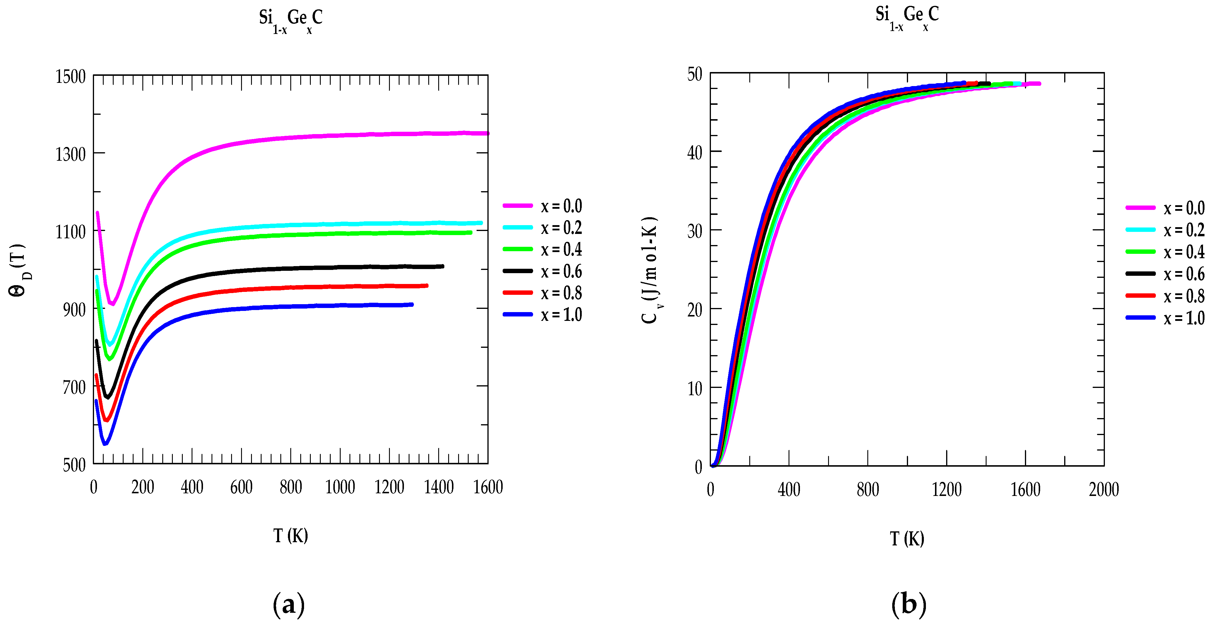
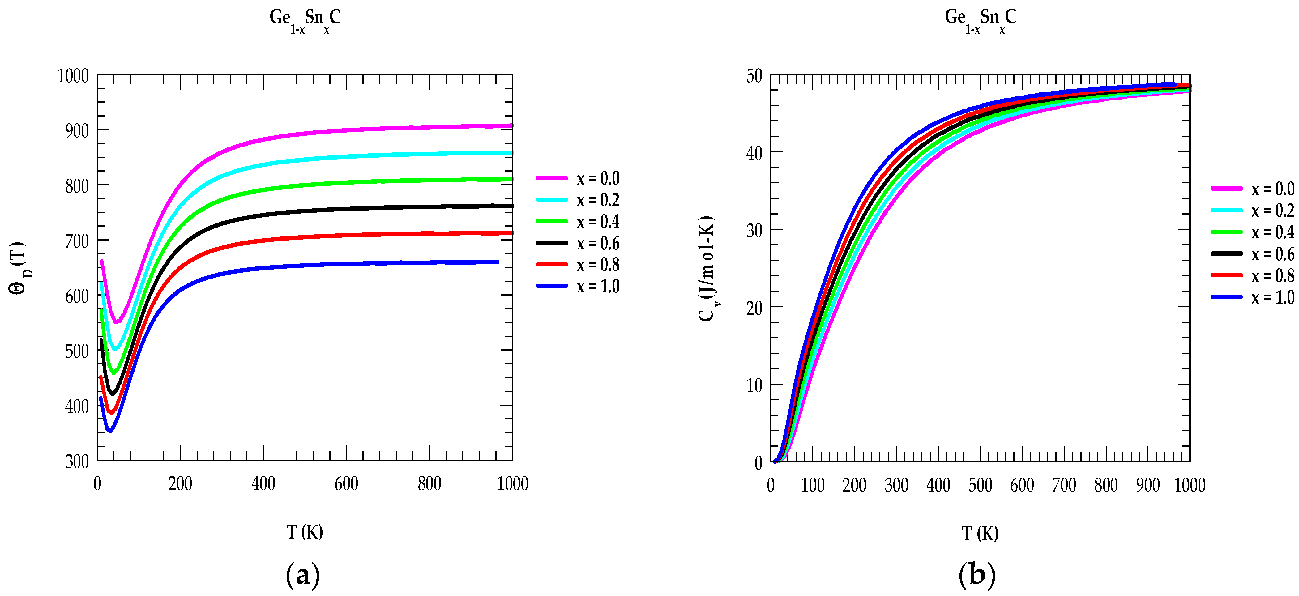
By using appropriate phonon dispersions and DOS, the x-dependent thermodynamic characteristics are simulated in the QHA for X1−xYxC ternary alloys between 0 < T < 1500 K. As an example, we have reported our results of ΘD(T) and Cv(T) for the Si1−xGexC alloys in Figure 7a and Figure 7b, respectively. Similar calculations have also been performed for other Si1−xSnxC (cf. Figure 8a,b) and Ge1−xSnxC (cf. Figure 9a,b) ternary alloys. From Figure 7a,b, some important noticeable facts can be justified. As x increases (from ≡0, 0.2, 0.4, 0.6, 0.8 and 1.0), the values of ΘD(T) [Cv(T)] decrease [increase] and in the limiting situations x → 0.0, and x →1.0, the results transform to those of SiC and GeC materials. Based on our simulations, the binary 3C-SiC has exhibited the highest ΘD(T) and lowest values. These results, related to its shorter bond-length and larger bond strength (see Table 2), can exhibit strong radiation tolerance with excellent resistance. Obviously, these characteristics have led to 3C-SiC being quite robust at higher T with less likelihood of breakdown in extreme conditions. We, therefore, feel that 3C-SiC is an ideal compound to be employed as a fuel-cladding material in nuclear reactors and high-temperature environments.
On the other hand, both GeC and SnC revealed significantly weaker bonding [149,150,151,152,153] (see Table 2) which instigated lower ΘD(T) and higher (T), values. Thus, we anticipate that these materials may not be suitable for fuel-cladding layers in nuclear reactors and/or in higher temperature environments. However, with a very small composition (x), the ternary Si1−xGexC alloys can still be deliberated. Both XC and X1−xYxC alloys have already been used to grow multilayer (viz., SiC/SiGe(Sn)C, GeC/Si(Ge)SnC) heterostructures. Thus, we feel that these structures may help engineers to design MQW/SL-based micro-/nanodevices for different strategic and civilian application needs.
3.2.3. Born Effective Charge for X1−xYxC Alloys
In polar materials, Born’s effective charge (also known as transverse or dynamic effective charge) manifests the coupling between lattice displacements and electrostatic fields. It is found that remains insensitive to the isotropic volume change but strongly affected by changes in the atomic positions associated with phase transitions (Pt). From a theoretical standpoint, in binary XC and ternary X1−xYxC alloys is important as Pt takes place due to the competition between long-range coulomb interactions and short-range forces. The long-range coulomb interactions are responsible for the observed splitting between and phonon frequencies. In Table 5, we have reported our simulated results of x-dependent and for X1−xYxC alloys. In the absence of data for ternary alloys, our theoretical results for the binary materials agree reasonably well with the experimental (for 3C-SiC) [107] and theoretical [123] results (for GeC and SnC) [122,124].
3.2.4. Fröhlich Coefficients
In semiconductors, the strength of the Fröhlich interaction is directly linked to the polar nature of its crystal lattice. In a highly polar material, the Coulomb field of a carrier (or exciton) couples more easily to the polar vibrations (i.e., phonons) of the crystal lattice, resulting in a strong Fröhlich coupling coefficient, . By using (cf. Equation (11)), the polaron effective mass can be calculated [154] in terms of the bare electron mass using the following expression:
where, the static and high-frequency values of the dielectric functions provide the means of quantifying the polar nature of materials, so that further insight into the Fröhlich interaction (see Equation (11)) can be gained via the dielectric characterizations.
It is to be noted that, except for 3C-SiC, no systematic calculations of the band structures and effective electron masses are known for the GeC and SnC materials. With Equation (11), and using the existing parameters (, , , ) for 3C-SiC from the literature [105,106,107], our calculation of (=0.576) has provided a value much higher than that reported by Adachi [130]. Interestingly, however, the calculation of polaron mass ( 0.243) using Equation (12) agrees very well with the theoretical result reported by Persson and Lindefelt [154]. Obviously, more experimental and theoretical efforts are needed for assessing the accurate values of the Fröhlich interaction coefficients for both the binary XC and ternary X1−xYxC alloys.
4. Discussions and Conclusions
In summary, we have used a realistic RIM and reported the results of our methodical simulations for comprehending the lattice dynamical and thermodynamic characteristics of zb (SiC, GeC, SnC) binary and (S1−xGexC, S1−xSnxC, Ge−xSnxC) ternary alloys. From a basic chemistry standpoint, one expects a gradual increase in the bond lengths (i.e., from Si-C → Ge-C → Sn-C) due to the differences in the sizes of the cations (Si, Ge, Sn) and (C) anion atoms. Accordingly, the increase in bond lengths will cause a decrease in their bond strengths. These facts are clearly revealed in our calculated IFCs of the RIM for XC materials (see Table 2), where the nearest-neighbor force constants [127] have shown steady decrease in their strength as one proceeds from SiC → GeC → SnC. Obviously, the atomic- and composition (x)-dependent variations in the bond strengths of mixed X1−xYxC alloys have instigated dramatic variations in the simulated RIM phonon dispersions and thermodynamic [e.g., ΘD(T), (T), traits.
In recent years, consistent efforts have been made using group-IV carbides and III-nitrides to develop devices for achieving efficient operations in challenging environments (viz., radiation, high-power, extreme temperature) where the electronic systems based on Si material have indicated weaknesses of survival. In this quest, it is necessary to assess the electronic and thermodynamic characteristics of XC materials to see if they satisfy the necessary requirements for their use in the high temperature/high power settings. One must note that the devices based on wide bandgap GaN and SiC have recently emerged in the commercial market for slowly replacing the traditional Si-built electronic parts. Both GaN and SiC materials with wide bandgaps, high critical electric fields, and low dielectric constants have reflected on the lower on-state resistance for a given blocking voltage. In addition, these materials have exhibited high Debye temperatures ΘD(T), low specific heats (T) and low thermal expansion coefficients. As compared to SiC, there are a few disadvantages for the selection of GaN material. The main problems have been identified as follows: (a) the manufacturing complexity, cost, intrinsic defects, and reliability concerns about the integration of GaN into the existing processes with limited availability of substrates, and (b) the relatively lower [higher] values of ΘD(T) [(T), [108,136]. Again, with respect to Si (≡ 1.12 eV), the reported theoretical bandgap energies of GeC and SnC materials are 1.51 eV [118], and 0.75 eV [117], respectively. Obviously, compared to SiC, the binary GeC, SnC and/or ternary Ge1−xSnxC alloys with lower and weaker bonding have exhibited different lattice dynamical and thermodynamic properties. Therefore, we strongly feel that devices based on binary GeC, SnC and/or Ge1−xSnxC materials may not be suitable for radiation detection in nuclear reactors or high-temperature, high-power settings. However, from recent successful efforts in the growth of ultrathin zb XC binary and X1−xYxC ternary alloys, along with their predicted results of phonon, structural, and thermodynamic traits, the materials can still be credible for the preparations of heterostructures in designing MQW and SL-based micro-/nanodevices for different strategic and civilian application needs.
Funding
This research has received no external funding.
Data Availability Statement
The data that support the findings of this study are available from the author upon reasonable request.
Acknowledgments
The author wishes to thank Deanne Snavely, Dean College of Natural Science and Mathematics at Indiana University of Pennsylvania (IUP), for the travel support and the Innovation Grant that he received from the School of Graduate Studies making this research possible.
Conflicts of Interest
The author declares having no financial and/or competing interests.
References
- Bell Telephone Laboratories, Inc. The Transistor: Selected Reference Material on Characteristics and Applications; Western Electric Co., Inc.: New York, NY, USA, 1951. [Google Scholar]
- Maram, R.; Kaushal, S.; Azaña, J.; Chen, L.R. Recent Trends and Advances of Silicon-Based Integrated Microwave Photonics. Photonics 2019, 6, 13. [Google Scholar] [CrossRef]
- Bennett, H.S.; Brederlow, R.; Costa, J.C.; Cottrell, P.E.; Huang, W.M.; Immorlica, A.A., Jr.; Mueller, J.-E.; Racanelli, M.; Shichijo, H.; Weitzel, C.E.; et al. Device and Technology Evolution for Si-Based RF Integrated Circuits. IEEE Trans. Electron Dev. 2005, 52, 1235. [Google Scholar] [CrossRef]
- Gutmann, R.J. Advanced Silicon IC Interconnect Technology and Design: Present Trends and RF Wireless Implications. IEEE Trans. Microwave Theory Tech. 1999, 47, 667–674. [Google Scholar] [CrossRef]
- Burghartz, J.N. Silicon RF technology—The two generic approaches. In Proceedings of the 27th European Solid-State Device Research Conference, Stuttgart, Germany, 22–24 September 1997; pp. 143–153. [Google Scholar]
- Razavi, B. CMOS technology characterization for analog and RF design. IEEE J. Solid-State Circuits 1999, 34, 268–276. [Google Scholar]
- Harame, D.; Comfort, J.; Cressler, J.; Crabbé, E.; Sun, J.; Meyerson, B.; Tice, T. Si/SiGe epitaxial base transistors, Parts I and II. IEEE Trans. Electron Dev. 1995, 42, 455–482. [Google Scholar] [CrossRef]
- Chen, D.; Li, R.; Xu, J.; Li, D.; Fei, C.; Yang, Y. Recent progress and development of radio frequency energy harvesting devices and circuits. Nano Energy 2023, 117, 108845. [Google Scholar] [CrossRef]
- Raut, P.; Nanda, U.; Panda, D.K. Review—Recent Trends on Junction-Less Field Effect Transistors in Terms of Device Topology, Modeling, and Application. ECS J. Solid Stat. Sci. Technol. 2023, 12, 031010. [Google Scholar] [CrossRef]
- Fu, Q.; Zhang, W.R.; Jin, D.Y.; Ding, C.B.; Zhao, Y.X.; Lu, D. Collector optimization for tradeoff between breakdown voltage and cut-off frequency in SiGe HBT. Chin. Phys. B 2014, 23, 114402. [Google Scholar] [CrossRef]
- Shahbaz, M.; Butt, M.A.; Piramidowicz, R. Breakthrough in Silicon Photonics Technology in Telecommunications, Biosensing, and Gas Sensing. Micromachines 2023, 14, 1637. [Google Scholar] [CrossRef]
- Kadri, E.; Messaoudi, O.; Krichen, M.; Dhahri, K.; Rasheed, M.; Dhahri, E.; Zouari, A.; Khirouni, K.; Barille, R. Optical and electrical properties of SiGe/Si solar cell heterostructures: Ellipsometric study. J. Alloys Compd. 2017, 721, 779–783. [Google Scholar] [CrossRef]
- Sun, Z.; Wang, L.; Luo, H.; Hamer, P.; Ye, H.; Hallam, B. Study of the Hydrogen Passivation Effect of Low-Temperature Deposited Amorphous Silicon Layers on SiGe Solar Cells Grown on a Silicon Substrate. ACS Appl. Energy Mater. 2023, 6, 12064–12071. [Google Scholar] [CrossRef]
- Ringel, S.A.; Carlin, J.; Andre, C.; Hudait, M.; Gonzalez, M.; Wilt, D.; Clark, E.; Jenkins, P.; Scheiman, D.; Allerman, A.; et al. Single-junction InGaP/GaAs solar cells grown on Si substrates with SiGe buffer layers. Prog. Photovolt. Res. Appl. 2002, 10, 417–426. [Google Scholar] [CrossRef]
- Erdtmann, M.; Carroll, M.; Vineis, C.; Badawi, H.; Bulsara, M.; Ringel, S. Growth and characterization of high-Ge content SiGe virtual substrates. Proc. Electrochem. Soc. 2003, 11, 106–117. [Google Scholar]
- Wang, L.; Conrad, B.; Soeriyadi, A.; Zhao, X.; Li, D.; Diaz, M.; Lochtefeld, A.; Gerger, A.; Perez-Wurfl, I.; Barnett, A. Current matched three-terminal dual junction GaAsP/SiGe tandem solar cell on Si. Sol. Energy Mater. Sol. Cells 2016, 146, 80–86. [Google Scholar] [CrossRef]
- Sankarasubramaniam, Y.; Akyildiz, I.E.; Mchughlin, S.W. Energy Efficiency based Packet Size Optimization in Wireless Sensor Networks. In Proceedings of the First IEEE International Workshop on Sensor Network Protocols and Applications, Anchorage, AK, USA, 11 May 2003. [Google Scholar] [CrossRef]
- Ojeda, F.; Mendez, D.; Fajardo, A.; Ellinger, F. On Wireless Sensor Network Models: A Cross-Layer Systematic Review. J. Sens. Actuator Netw. 2023, 12, 50. [Google Scholar] [CrossRef]
- Xing, J.; Sun, C.; Xiong, B.; Wang, J.; Hao, Z.; Wang, L.; Han, Y.; Li, H.; Luo, Y. Membrane multiple quantum-well electro-optical modulator employing low loss high-k radio-frequency slot waveguides. Opt. Express 2022, 30, 23260. [Google Scholar] [CrossRef] [PubMed]
- Zhao, X.; Xiong, B.; Sun, C.; Luo, Y. Low drive voltage optical phase modulator with novel InGaAlAs/InAlAs multiple-quantum-barrier based n-i-n heterostructure. Opt. Express 2013, 21, 24894–24903. [Google Scholar] [CrossRef] [PubMed]
- Liu, X.; Xiong, B.; Sun, C.; Wang, J.; Hao, Z.; Wang, L.; Han, Y.; Li, H.; Yu, J.; Luo, Y. Wideband thin-film lithium niobate modulator with low half-wave-voltage length product. Chin. Opt. Lett. 2021, 19, 060016. [Google Scholar] [CrossRef]
- Xing, J.; Sun, C.; Xiong, B.; Wang, J.; Hao, Z.; Wang, L.; Han, Y.; Li, H.; Yu, J.; Luo, Y. Low loss hybrid plasmon polariton Mach-Zehnder modulators. OSA Contin. 2021, 4, 2721–2733. [Google Scholar] [CrossRef]
- Fujii, T.; Hiraki, T.; Aihara, T.; Nishi, H.; Takeda, K.; Sato, T.; Kakitsuka, T.; Tsuchizawa, T.; Matsuo, S. Development of an Epitaxial Growth Technique Using III-V on a Si Platform for Heterogeneous Integration of Membrane Photonic Devices on Si. Appl. Sci. 2021, 11, 1801. [Google Scholar] [CrossRef]
- Rickman, A. The commercialization of silicon photonics. Nat. Photonics 2014, 8, 579–582. [Google Scholar] [CrossRef]
- Nagarajan, R.; Joyner, C.H.; Schneider, R.P.; Bostak, J.S.; Butrie, T.; Dentai, A.G.; Dominic, V.G.; Evans, P.W.; Kato, M.; Kauffman, M.; et al. Large-scale photonic integrated circuits. IEEE J. Sel. Top. Quantum Electron. 2005, 11, 50–65. [Google Scholar] [CrossRef]
- Komljenovic, T.; Davenport, M.; Hulme, J.; Liu, A.Y.; Santis, C.T.; Spott, A.; Srinivasan, S.; Stanton, E.J.; Zhang, C.; Bowers, J.E. Heterogeneous Silicon Photonic Integrated Circuits. J. Light. Technol. 2016, 34, 20–35. [Google Scholar] [CrossRef]
- Dong, P.; Liu, X.; Chandrasekhar, S.; Buhl, L.L.; Aroca, R.; Chen, Y.-K. Monolithic Silicon Photonic Integrated Circuits for Compact 100+Gb/s Coherent Optical Receivers and Transmitters. IEEE J. Sel. Top. Quantum Electron. 2014, 20, 150–157. [Google Scholar] [CrossRef]
- Horikawa, T.; Shimura, D.; Okayama, H.; Jeong, S.-H.; Takahashi, H.; Ushida, J.; Sobu, Y.; Shiina, A.; Tokushima, M.; Kinoshita, K.; et al. A 300-mm Silicon Photonics Platform for Large-Scale Device Integration. IEEE J. Sel. Top. Quantum Electron. 2018, 24, 1–15. [Google Scholar] [CrossRef]
- Kukushkin, S.; Osipov, A.; Redkov, A. SiC/Si as a New Platform for Growth of Wide-Bandgap Semiconductors. In Mechanics and Control of Solids and Structures; Polyanskiy, V.A., Belyaev, A.K., Eds.; Advanced Structured Materials; Springer Nature: Cham, Switzerland, 2022; Chapter 18; p. 164. [Google Scholar]
- Nguyen, T.-K.; Yadav, S.; Truong, T.-A.; Han, M.; Barton, M.; Leitch, M.; Guzman, P.; Dinh, T.; Ashok, A.; Vu, H.; et al. Integrated, Transparent Silicon Carbide Electronics and Sensors for Radio Frequency Biomedical Therapy. ACS Nano 2022, 16, 10890–10903. [Google Scholar] [CrossRef] [PubMed]
- Pham, T.A.; Nguyen, T.K.; Vadivelu, R.K.; Dinh, T.; Qamar, A.; Yadav, S.; Yamauchi, Y.; Rogers, J.A.; Nguyen, N.T.; Phan, H.P. Stretchable Bioelectronics: A Versatile Sacrificial Layer for Transfer Printing of Wide Bandgap Materials for Implantable and Stretchable Bioelectronics. Adv. Funct. Mater. 2020, 30, 2070287. [Google Scholar] [CrossRef]
- Nguyen, T.K.; Phan, H.P.; Kamble, H.; Vadivelu, R.; Dinh, T.; Iacopi, A.; Walker, G.; Hold, L.; Nguyen, N.T.; Dao, D.V. Superior Robust Ultrathin Single-Crystalline Silicon Carbide Membrane as a Versatile Platform for Biological Applications. ACS Appl. Mater. Interfaces 2017, 9, 41641–41647. [Google Scholar] [CrossRef] [PubMed]
- Yang, H.; Ma, Y.; Da, Y. Progress of structural and electronic properties of diamond: A mini review. Funct. Diam. 2021, 1, 150–159. [Google Scholar] [CrossRef]
- Yue, Y.; Gao, Y.; Hu, W.; Xu, B.; Wang, J.; Zhang, X.; Zhang, Q.; Wang, Y.; Ge, B.; Yang, Z.; et al. Hierarchically structured diamond composite with exceptional Toughness. Nature 2020, 582, 370–374. [Google Scholar] [CrossRef]
- Huang, Q.; Yu, D.; Xu, B.; Hu, W.; Ma, Y.; Wang, Y.; Zhao, Z.; Wen, B.; He, J.; Liu, Z.; et al. Nanotwinned diamond with unprecedented hardness and stability. Nature 2014, 510, 250–253. [Google Scholar] [CrossRef]
- Ekimov, E.A.; Sidorov, V.A.; Bauer, E.D.; Mel’Nik, N.N.; Curro, N.J.; Thompson, J.D.; Stishov, S.M. Superconductivity in diamond. Nature 2004, 428, 542–545. [Google Scholar] [CrossRef] [PubMed]
- Bauer, M.R.; Tolle, J.; Bungay, C.; Chizmeshya, A.V.G.; Smith, D.J.; Menéndez, J.; Kouvetakis, J. Tunable band structure in diamond–cubic tin–germanium alloys grown on silicon substrates. Solid State Commun. 2003, 127, 355–359. [Google Scholar] [CrossRef]
- Islam, M.S.; Mojumder, R.H.; Hassan, A.; Sohag, M.U.; Park, J. High-Efficiency Multi Quantum Well Blue LED Using 2D-SiC as an Active Material. In Proceedings of the 2021 5th International Conference on Electrical Engineering and Information & Communication Technology (ICEEICT), Dhaka, Bangladesh, 18–20 November 2021. [Google Scholar]
- Zhang, L.; Cui, Z. Theoretical Study on Electronic, Magnetic and Optical Properties of Non-Metal Atoms Adsorbed onto Germanium Carbide. Nanomaterials 2022, 12, 1712. [Google Scholar] [CrossRef] [PubMed]
- Mélinon, P.; Masenelli, B.; Tournus, F.; Perez, A. Playing with carbon and silicon at the nanoscale. Nat. Mater. 2007, 6, 479–490. [Google Scholar] [CrossRef] [PubMed]
- Polyanskiy, V.A.; Belyaev, A.K. (Eds.) Mechanics and Control of Solids and Structures, Advanced Structured Materials; Springer Nature: Cham, Switzerland, 2022; p. 164. Available online: https://link.springer.com/bookseries/8611 (accessed on 27 February 2024).
- Ikoma, Y.; Endo, T.; Watanabe, F.; Motooka, T. Growth of Ultrathin Epitaxial 3C-SiC Films on Si(100) by Pulsed Supersonic Free Jets of CH3SiH3. Jpn. J. Appl. Phys. 1999, 38, L301. [Google Scholar] [CrossRef]
- Ikoma, Y.; Endo, T.; Watanabe, F.; Motooka, T. Growth of Si/3C–SiC/Si(100) heterostructures by pulsed supersonic free jets. Appl. Phys. Lett. 1999, 75, 3977–3979. [Google Scholar] [CrossRef]
- Ohtani, R.; Ikoma, Y.; Motooka, T. Formation of Si/SiC heterostructures for silicon-based quantum devices using single CH3SiH3-gas source free jet. Mater. Res. Soc. Symp. Proc. 2004, 815, J5.11.1. [Google Scholar] [CrossRef]
- Yoshimura, S.; Sugimoto, S.; Takeuchi, T.; Murai, K.; Kiuchi, M. Low energy Si+, SiCH5+, or C+ beam injections to silicon substrates during chemical vapor deposition with dimethyl silane. Heliyon 2023, 9, e19002. [Google Scholar] [CrossRef] [PubMed]
- Gallagher, J.D.; Senaratne, C.L.; Kouvetakis, J.; Menéndez, J. Compositional dependence of the bowing parameter for the direct and indirect band gaps in Ge 1-y Sn y alloys. Appl. Phys. Lett. 2014, 105, 142102. [Google Scholar] [CrossRef]
- Ghetmiri, S.A.; Du, W.; Margetis, J.; Mosleh, A.; Cousar, L.; Conley, B.R.; Domulevicz, L.; Nazzal, A.; Sun, G.; Soref, R.A.; et al. Direct-bandgap GeSn grown on silicon with 2230 nm photoluminescence. Appl. Phys. Lett. 2014, 105, 151109. [Google Scholar] [CrossRef]
- Wirths, S.; Geiger, R.; von den Driesch, N.; Mussler, G.; Stoica, T.; Mantl, S.; Ikonic, Z.; Luysberg, M.; Chiussi, S.; Hartmann, J.M.; et al. Lasing in direct-bandgap GeSn alloy grown on Si. Nat. Photonics 2015, 9, 88–92. [Google Scholar] [CrossRef]
- Xu, Z.; Li, Y.; Liu, Z. Controlling electronic and optical properties of layered SiC and GeC sheets by strain engineering. Mater. Des. 2016, 108, 333–342. [Google Scholar] [CrossRef]
- Xua, Q.; Cai, W.; Li, W.; Sreeprasad, T.S.; He, Z.; Ong, W.-J.; Li, N. Two-dimensional quantum dots: Fundamentals, photoluminescence mechanism and their energy and environmental applications. Mater. Today Energy 2018, 10, 222–240. [Google Scholar] [CrossRef]
- Schulte-Braucks, C.; Glass, S.; Hofmann, E.; Stange, D.; von den Driesch, N.; Hartmann, J.M.; Ikonic, Z.; Zhao, Q.T.; Buca, D.; Mantl, S. Process modules for GeSn nanoelectronics with high Sn-contents. Solid-State Electron. 2017, 128, 54–59. [Google Scholar] [CrossRef]
- Shen, Z.; Chen, J.; Li, B.; Li, G.; Zheng, H.; Men, J.; Hou, X. Tunable fabrication and photoluminescence property of SiC nano wires with different microstructures. Appl. Surf. Sci. 2020, 506, 144979. [Google Scholar] [CrossRef]
- Dey, T.; Reza, M.S.; Arbogast, A.W.; Holtz, M.; Droopad, R.; Bank, S.R.; Wistey, M.A. Molecular beam epitaxy of highly crystalline GeSnC using CBr4 at low temperatures. Appl. Phys. Lett. 2022, 121, 122104. [Google Scholar] [CrossRef]
- Dey, T.; Arbogast, A.W.; Meng, Q.; Reza, M.S.; Muhowski, A.J.; Cooper, J.P.; Ozdemir, E.; Naab, F.U.; Borrely, T.; Anderson, J.; et al. Influence of H on Sn incorporation in GeSnC alloys grown using molecular beam epitaxy. J. Appl. Phys. 2023, 134, 193102. [Google Scholar] [CrossRef]
- Giunto, A.; Morral, A.F.I. The GeSn Alloy and its Optoelectronic Properties: A Critical Review of the Current Understanding. arXiv 2023, arXiv:2309.10584. [Google Scholar] [CrossRef]
- Cardoux, C.; Casiez, L.; Pauc, N.; Calvo, V.; Coudurier, N.; Rodriguez, P.; Richy, J.; Barritault, P.; Lartigue, O.; Constancias, C.; et al. Room temperature spectral characterization of direct band gap Ge0.85Sn0.15 LEDs and photodiodes. In Proceedings of the 2022 Proceedings SPIE OPTO, Silicon Photonics XVII, San Francisco, CA, USA, 22–27 January 2022; p. 120060A. [Google Scholar] [CrossRef]
- Moutanabbir, O.; Assali, S.; Gong, X.; O’Reilly, E.; Broderick, C.A.; Marzban, B.; Witzens, J.; Du, W.; Yu, S.-Q.; Chelnokov, A.; et al. Monolithic infrared silicon photonics: The rise of (Si)GeSn semiconductors. Appl. Phys. Lett. 2021, 118, 110502. [Google Scholar] [CrossRef]
- Atalla, M.R.M.; Assali, S.; Koelling, S.; Attiaoui, A.; Moutanabbir, O. High-Bandwidth Extended-SWIR GeSn Photodetectors on Silicon Achieving Ultrafast Broadband Spectroscopic Response. ACS Photonics 2022, 9, 1425–1433. [Google Scholar] [CrossRef]
- Simola, E.T.; Kiyek, V.; Ballabio, A.; Schlykow, V.; Frigerio, J.; Zucchetti, C.; De Iacovo, A.; Colace, L.; Yamamoto, Y.; Capellini, G.; et al. CMOS-Compatible Bias-Tunable Dual-Band Detector Based on GeSn/Ge/Si Coupled Photodiodes. ACS Photonics 2021, 8, 2166–2173. [Google Scholar] [CrossRef]
- Tran, H.; Pham, T.; Margetis, J.; Zhou, Y.; Dou, W.; Grant, P.C.; Grant, J.M.; Al-Kabi, S.; Sun, G.; Soref, R.A.; et al. Si-Based GeSn Photodetectors toward MidInfrared Imaging Applications. ACS Photonics 2019, 6, 2807–2815. [Google Scholar] [CrossRef]
- Zhang, D.; Hu, X.; Liu, D.; Lin, X.; Wang, W.; Ding, Z.; Wang, Z.; Cheng, B.; Xue, C. GeSn on Si avalanche photodiodes for short wave infrared detection. In Optical Sensing and Imaging Technologies and Applications; Liu, D., Gong, H., Guina, M., Lu, J., Eds.; SPIE: Bellingham, WA, USA, 2018; p. 54. [Google Scholar]
- Kim, Y.; Assali, S.; Burt, D.; Jung, Y.; Joo, H.-J.; Chen, M.; Ikonic, Z.; Moutanabbir, O.; Nam, D. Improved GeSn microdisk lasers directly sitting on Si. In Silicon Photonics XVII; Reed, G.T., Knights, A.P., Eds.; SPIE: Bellingham, WA, USA, 2022; p. 21. [Google Scholar]
- Ojo, S.; Zhou, Y.; Acharya, S.; Saunders, N.; Amoah, S.; Jheng, Y.-T.; Tran, H.; Du, W.; Chang, G.-E.; Li, B.; et al. Silicon-based electrically injected GeSn lasers. In Physics and Simulation of Optoelectronic Devices XXX; Osinski, M., Arakawa, Y., Witzigmann, B., Eds.; SPIE: Bellingham, WA, USA, 2022; p. 15. [Google Scholar]
- Marzban, B.; Seidel, L.; Liu, T.; Wu, K.; Kiyek, V.; Zoellner, M.H.; Ikonic, Z.; Schulze, J.; Grutzmacher, D.; Capellini, G.; et al. Strain Engineered Electrically Pumped SiGeSn Microring Lasers on Si. ACS Photonics 2023, 10, 217–224. [Google Scholar] [CrossRef]
- Kasper, E.; Herzog, H.J.; Kibbel, H. A one-dimensional SiGe superlattice grown by UHV epitaxy. Appl. Phys. 1975, 8, 199–205. [Google Scholar] [CrossRef]
- Iyer, S.S.; Patton, G.L.; Delage, S.S.; Tiwari, S.; Stork, J.M.C. Silicon-germanium base heterojunction bipolar transistors by molecular beam epitaxy. In Proceedings of the International Electron Devices Meeting, IEDM Technical Digest, Washington, DC, USA, 6–9 December 1987; p. 874. [Google Scholar]
- Okinaka, M.; Hamana, Y.; Tokuda, T.; Ohta, J.; Nunoshita, M. MBE growth mode and C incorporation of GeC epilayers on Si(0 0 1) substrates using an arc plasma gun as a novel C source. J. Cryst. Growth 2003, 249, 78–86. [Google Scholar] [CrossRef]
- Lu, H.; Liu, W.; Wang, H.; Liu, X.; Zhang, Y.; Yang, D.; Pi, X. Molecular beam epitaxy growth and scanning tunneling microscopy study of 2D layered materials on epitaxial graphene/silicon carbide. Nanotechnology 2023, 34, 132001. [Google Scholar] [CrossRef] [PubMed]
- Islam, M.R.; Islam, M.S.; Mitul, A.F.; Mojumder, M.R.H.; Jannatul, A.S.M.; Islam, C.S.; Park, J. Superior tunable photocatalytic properties for water splitting in two dimensional GeC/SiC van der Waals hetero bilayers. Sci. Rep. 2021, 11, 17739. [Google Scholar] [CrossRef] [PubMed]
- Tayaba, S.; Sethi, H.; Shahid, H.; Malik, R.; Ikram, M.; Ali, S.; Khaliq, S.; Khan, Q.; Maqbool, M. Silicon-Germanium and carbon-based superconductors for electronic, industrial, and medical applications. Mater. Sci. Eng. B 2023, 290, 116332. [Google Scholar] [CrossRef]
- Bean, J.C. Silicon based semiconductor heterostructures: Column IV bandgap engineering. Proc. IEEE 1992, 80, 571–587. [Google Scholar] [CrossRef]
- Li, X.; Jacobson, H.; Boulle, A.; Chaussende, D.; Henry, A. Double-Position-Boundaries Free 3C-SiC Epitaxial Layers Grown on On-Axis 4H-SiC. ECS J. Solid State Sci. Technol. 2014, 3, P75. [Google Scholar] [CrossRef]
- Xin, B.; Jia, R.X.; Hu, J.C.; Tsai, C.Y.; Lin, H.H.; Zhang, Y.M. A step-by-step experiment of 3C-SiC hetero-epitaxial growth on 4H-SiC by CVD. Appl. Surf. Sci. 2015, 357, 985–993. [Google Scholar] [CrossRef]
- Wu, J.; Qian, S.T.; Huo, T.G.; Zheng, J.X.; Zhang, P.L.; Dai, Y.; Geng, D.S. Effect of PyC Inner Coating on Preparation of 3C-SiC Coating on Quartz Glass by Chemical Vapor Reaction. Front. Mater. 2022, 9, 897900. [Google Scholar] [CrossRef]
- Kaloyeros, A.E.; Arkles, B. Silicon Carbide Thin Film Technologies: Recent Advances in Processing, Properties, and Applications—Part I Thermal and Plasma CVD. ECS J. Solid State Sci. Technol. 2023, 12, 103001. [Google Scholar] [CrossRef]
- Hartmanna, J.M.; Abbadiea, A.; Vineta, M.; Claveliera, L.; Holligera, P.; Lafonda, D.; Semeria, M.N.; Gentile, P. Growth kinetics of Si on fullsheet, patterned and silicon-on-insulator substrates. J. Cryst. Growth 2003, 257, 19–30. [Google Scholar] [CrossRef]
- Lukin, D.M.; Guidry, M.A.; Vučković, J. Silicon Carbide: From Abrasives to Quantum Photonics. Opt. Photonics News 2021, 32, 34–41. [Google Scholar] [CrossRef]
- La Via, F.; Camarda, M.; La Magna, A. Mechanisms of growth and defect properties of epitaxial SiC. Appl. Phys. Rev. 2014, 1, 031301. [Google Scholar] [CrossRef]
- Fraga, M.A.; Bosi, M.; Negri, N. Silicon carbide in microsystem technology—Thin film vs bulk material. In Advanced Silicon Carbide Devices and Processing; Saddow, S.E., La Via, F., Eds.; IntechOpen: London, UK, 2015; Chapter 1; p. 3. [Google Scholar]
- Ou, H.; Shi, X.; Lu, Y.; Kollmuss, M.; Steiner, J.; Tabouret, V.; Syväjärvi, M.; Wellmann, P.; Chaussende, D. Novel photonic applications of silicon carbide. Materials 2023, 16, 1014. [Google Scholar] [CrossRef]
- Kaloyeros, A.E.; Jové, F.A.; Goff, J.; Arkles, B. Silicon nitride and silicon nitride-rich thin film technologies: Trends in deposition techniques and related applications. ECS J. Solid State Sci. Technol. 2017, 6, P691. [Google Scholar] [CrossRef]
- Kaloyeros, A.E.; Pan, Y.; Goff, J.; Arkles, B. Review—Silicon nitride and silicon nitride-rich thin film technologies: State-of-the-art processing technologies, properties, and applications. ECS J. Solid State Sci. Technol. 2020, 9, 062006. [Google Scholar] [CrossRef]
- Marsi, N.; Majlis, B.Y.; Hamzah, A.; Mohd-Yasin, F. High reliability of MEMS packaged capacitive pressure sensor employing 3C-SiC for high temperature. Energy Procedia 2015, 68, 471–479. [Google Scholar] [CrossRef]
- Feller, T.; Rosenfeldt, S.; Retsch, M. Carbothermal synthesis of micron-sized, uniform, spherical silicon carbide (SiC) particles. Z. Anorg. Allg. Chem. 2021, 647, 2172–2180. [Google Scholar] [CrossRef]
- Kawanishi, S.; Daikoku, H.; Shibata, H.; Yoshikawa, T. Suppressing solvent compositional change during solution growth of SiC using SiC/C gradient crucible. J. Cryst. Growth 2021, 576, 126382. [Google Scholar] [CrossRef]
- Sannodo, N.; Osumi, A.; Kaminaga, K.; Maruyama, S.; Matsumoto, Y. Vapor-liquid-solid-like growth of high-quality and uniform 3C-SiC heteroepitaxial films on alpha-Al2O3 (0001) substrates. CrystEngComm 2021, 23, 1709–1717. [Google Scholar] [CrossRef]
- Kukushkin, S.A.; Osipov, A.V. Epitaxial silicon carbide on silicon. method of coordinated substitution of atoms (a review). Russ. J. Gen. Chem. 2022, 92, 584–610. [Google Scholar] [CrossRef]
- Majid, A. A perspective on non-stoichiometry in silicon carbide (review article). Ceram. Int. 2018, 44, 1277–1283. [Google Scholar] [CrossRef]
- Spera, M.; Greco, G.; Lo Nigro, R.; Bongiorno, C.; Giannazzo, F.; Zielinski, M.; La Via, F.; Roccaforte, F. Ohmic contacts on n-type and p-type cubic silicon carbide (3C-SiC) grown on silicon. Mater. Sci. Semicond. Process. 2019, 93, 295–298. [Google Scholar] [CrossRef]
- Galashev, A.Y.; Abramova, K.A. Computer simulation of obtaining thin films of silicon carbide. Phys. Chem. Chem. Phys. 2023, 25, 3834–3847. [Google Scholar] [CrossRef] [PubMed]
- Smith, D.J.; Todd, M.; McMurran, J.; Kouvetakis, J. Structural properties of heteroepitaxial germanium carbon alloys grown on (100) Si. Philos. Mag. A 2001, 81, 1613–1624. [Google Scholar] [CrossRef]
- Schuh, P.; Scholer, M.; Wilhelm, M.; Syvajarvi, M.; Litrico, G.; La Via, F.; Mauceri, M.; Wellmann, P.J. Sublimation growth of bulk 3C-SiC using 3C-SiC-on-Si (100) seeding layers. J. Cryst. Growth 2017, 478, 159–162. [Google Scholar] [CrossRef]
- Ha, C.V.; Ha, L.T.; Hue, D.T.; Nguyen, D.K.; Anh, D.T.; Sanchezd, J.G.; Hoat, D.M. First-principles study of SiC and GeC monolayers with adsorbed non-metal atoms. RSC Adv. 2023, 13, 14879–14886. [Google Scholar] [CrossRef]
- Werninghaus, T.; Friedrich, M.; Cimalla, V.; Scheiner, J.; Goldhahn, R.; Zahn, D.R.T.; Pezold, J. Optical characterization of MBE grown cubic and hexagonal SiC films on Si(111). Diam. Relat. Mater. 1998, 7, 1385–1389. [Google Scholar]
- Yasui, K.; Narita, Y.; Inubushi, T.; Akahane, T. In situ observation of reflection high-energy electron diffraction during the initial growth of SiC on Si using dimethylsilane. J. Cryst. Growth 2002, 237–239, 1254–1259. [Google Scholar] [CrossRef]
- Kosiba, R.; Liday, J.; Ecke, G.; Ambacher, O.; Breza, J.; Vogrincic, P. Quantitative Auger electron spectroscopy of SiC. Vacuum 2006, 80, 990–995. [Google Scholar] [CrossRef]
- Zhao, S.; Chen, J.; Yang, S.; Yan, G.; Shen, Z.; Zhao, W.; Wang, L.; Liu, X.; Sun, G.; Zeng, Y. Effect of temperature on growth of epitaxial layer on semi-insulating 4H-SiC substrate. J. Cryst. Growth 2023, 603, 127008. [Google Scholar] [CrossRef]
- Tang, Z.; Gu, L.; Ma, H.; Dai, K.; Luo, Q.; Zhang, N.; Huang, J.; Fan, J. Study on the Surface Structure of N-Doped 4H-SiC Homoepitaxial Layer Dependence on the Growth Temperature and C/Si Ratio Deposited by CVD. Crystals 2023, 13, 193. [Google Scholar] [CrossRef]
- Sreelakshmi, N.; Umapathy, G.R.; Abhaya, S.; David, C.; Ojha, S.; Amirthapandian, S. Ionization-induced annealing of defects in 3C–SiC: Ion channeling and positron annihilation spectroscopy investigations. J. Mater. Res. 2023, 38, 1349–1362. [Google Scholar] [CrossRef]
- Bayu Aji, L.B.; Stavrou, E.; Wallace, J.B.; Boulle, A.; Debelle, A.; Kucheyev, S.O. Comparative study of radiation defect dynamics in 3C-SiC by X-ray diffraction, Raman scattering, and ion channeling. Appl. Phys. A 2019, 125, 28. [Google Scholar] [CrossRef]
- Boulle, A.; Debelle, A.; Wallace, J.B.; Aji, L.B.; Kucheyev, S.O. The amorphization of 3C-SiC irradiated at moderately elevated temperatures as revealed by X-ray diffraction. Acta Mater. 2017, 140, 250–257. [Google Scholar] [CrossRef]
- Zhang, L.; Jiang, W.; Pan, C.; Fadanelli, R.C.; Ai, W.; Chen, L.; Wang, T. Raman study of amorphization in nanocrystalline 3C–SiC irradiated with C+ and He+ ions. J. Raman Spectrosc. 2019, 50, 1197–1204. [Google Scholar] [CrossRef]
- Lindner, J.K.N.; Tsang, W.M.; Wong, S.P.; Xu, J.B.; Wilson, I.H. XTEM characterization of tungsten implanted SiC thin films on silicon for field emission devices. Thin Solid Films 2003, 427, 417–421. [Google Scholar] [CrossRef]
- Scuderi, V.; Calabretta, C.; Anzalone, R.; Mauceri, M.; La Via, F. Characterization of 4H- and 6H-Like Stacking Faults in Cross Section of 3C-SiC Epitaxial Layer by Room-Temperature µ-Photoluminescence and µ-Raman Analysis. Materials 2020, 13, 1837. [Google Scholar] [CrossRef]
- Feldman, D.W.; Parker, J.H., Jr.; Choyke, W.J.; Patrick, L. Phonon Dispersion Curves by Raman Scattering in SiC, Polytypes 3C, 4H, 6H, 15R, and 21R. Phys. Rev. 1968, 173, 787. [Google Scholar] [CrossRef]
- Yoshida, M.; Onodera, A.; Ueno, M.; Takemura, K.; Shimomura, O. Pressure-induced phase transition in SiC. Phys. Rev. B 1993, 48, 10587. [Google Scholar] [CrossRef] [PubMed]
- Olego, D.; Cardona, M.; Vogl, P. Pressure dependence of the optical phonons and transverse effective charge in 3C-SiC. Phys. Rev. B 1982, 25, 3878. [Google Scholar] [CrossRef]
- Talwar, D.N. Spectroscopic Investigations for the Dynamical Properties of Defects in Bulk and Epitaxially Grown 3C-SiC/Si (100). In Handbook of Silicon Carbide Materials and Devices; Feng, Z.C., Ed.; CRC Press: Boca Raton, FL, USA, 2023; Chapter 3. [Google Scholar]
- Sahin, H.; Cahangirov, S.; Topsakal, M.; Bekaroglu, E.; Akturk, E.; Senge, R.T.; Ciraci, S. Monolayer honeycomb structures of group-IV elements and III-V binary compounds: First-principles calculations. Phys. Rev. B 2009, 80, 155453. [Google Scholar] [CrossRef]
- Lin, S.S. Light-emitting two-dimensional ultrathin silicon carbide. J. Phys. C 2012, 116, 3951–3955. [Google Scholar] [CrossRef]
- Jankousky, M.; Garrity, E.M.; Stevanovic, V. Polymorphism of group-IV carbides: Structures, (meta)stability, electronic, and transport properties. Phys. Rev. Mater. 2023, 7, 053606. [Google Scholar] [CrossRef]
- Karch, K.; Bechstedt, F.; Pavone, P.; Strauch, D. Pressure-dependent properties of SiC polytypes. Phys. Rev. B 1996, 53, 13400. [Google Scholar] [CrossRef]
- Miao, M.S.; Prikhodko, M.; Lambrecht, W.R.L. Changes of the geometry and band structure of SiC along the orthorhombic high-pressure transition path between the zinc-blende and rocksalt structures. Phys. Rev. B 2002, 66, 064107. [Google Scholar] [CrossRef]
- Jiang, J.; Zheng, W.; Xiao, H.Y.; Liu, Z.J.; Zu, X.T. A comparative study of the mechanical and thermal properties of defective ZrC, TiC and SiC. Sci. Rep. 2017, 7, 9344. [Google Scholar] [CrossRef]
- Lu, Y.P.; Wei, H.D.; Zhu, J.; Yang, X.D. First-principles study of pressure-induced phase transition in silicon carbide. Physica B 2008, 403, 3543–3546. [Google Scholar] [CrossRef]
- Hao, A.; Yang, X.C.; Wang, X.M.; Zhu, Y.; Liu, X.; Liu, R.P. First-principles investigations on electronic, elastic, and optical properties of XC (X = Si, Ge, and Sn) under high pressure. J. Appl. Phys. 2010, 108, 063531. [Google Scholar] [CrossRef]
- Pandey, R.; Rérat, M.; Darrigan, C.; Causà, M. A theoretical study of stability, electronic, and optical properties of GeC and SnC. J. Appl. Phys. 2000, 88, 6462–6466. [Google Scholar] [CrossRef]
- Khenata, R.; Baltache, H.; Sahnoun, M.; Driz, M.; Rérat, M.; Abbar, B. Full potential linearized augmented plane wave calculations of structural and electronic properties of GeC, SnC and GeSn. Physica B 2003, 336, 321–328. [Google Scholar] [CrossRef]
- Sekkal, W.; Zaoui, A. Predictive study of thermodynamic properties of GeC. New J. Phys. 2002, 4, 9. [Google Scholar] [CrossRef]
- Varshney, D.; Shriya, S.; Varshney, M.; Singh, N.; Khenata, R. Elastic and thermo-dynamical properties of cubic (3C) silicon carbide under high pressure and high temperature. J. Theor. Appl. Phys. 2015, 9, 221–249. [Google Scholar] [CrossRef]
- Karch, K.; Bechstedt, F.; Pavone, P.; Strauch, D. Pressure-dependent dynamical and dielectric properties of cubic SiC. J. Phys. Condens. Matter 1996, 8, 2945. [Google Scholar] [CrossRef]
- Karch, K.; Pavone, P.; Windl, W.; Schütt, O.; Strauch, D. Ab initio calculation of structural and lattice-dynamical properties of silicon carbide. Phys. Rev. B 1994, 50, 17054. [Google Scholar] [CrossRef]
- Wang, C.Z.; Yu, R.C.; Krakauer, H. Pressure dependence of Born effective charges, dielectric constant, and lattice dynamics in SiC. Phys. Rev. B 1996, 53, 5430. [Google Scholar] [CrossRef] [PubMed]
- Souadkia, M.; Bennecer, B.; Kalarasse, F. Elastic, vibrational and thermodynamic properties of α-Sn based group IV semiconductors and GeC under pressure. J. Phys. Chem. Solids 2013, 74, 1615–1625. [Google Scholar] [CrossRef]
- Zhang, X.; Quan, S.; Ying, C.; Li, Z. Theoretical investigations on the structural, lattice dynamical and thermodynamic properties of XC (X = Si, Ge, Sn). Solid State Commun. 2011, 151, 1545–1549. [Google Scholar] [CrossRef]
- Zhang, P.; Crespi, V.H.; Chang, E.; Louie, S.G.; Cohen, M.L. Theory of metastable group-IV alloys formed from CVD precursors. Phys. Rev. B 2001, 64, 235201. [Google Scholar] [CrossRef]
- Kunc, K. Dynamique de réseau de composés ANB8-N présentant la structure de la blende. Ann. Phys. 1973, 8, 319–401. [Google Scholar]
- Plumelle, P.; Vandevyver, M. Lattice dynamics of ZnTe and CdTe. Phys. Stat. Sol. 1976, 73, 271–281. [Google Scholar] [CrossRef]
- Serrano, J.; Strempfer, J.; Cardona, M.; Schwoerer-Böhning, M.; Requardt, H.; Lorenzen, M.; Stojetz, B.; Pavone, P.; Choyke, W.J. Determination of the phonon dispersion of zinc blende (3C) silicon carbide by inelastic X-ray scattering. Appl. Phys. Lett. 2002, 80, 4360–4362. [Google Scholar] [CrossRef]
- Adachi, S. Properties of Semiconductor Alloys: Group-IV, III–V and II–VI, Semiconductors; Wiley: Hoboken, NJ, USA, 2009. [Google Scholar]
- Kutty, A.P.G. Phonons in mixed crystals. Solid State Commun. 1974, 14, 213–215. [Google Scholar] [CrossRef]
- Talwar, D.N. On the pressure-dependent phonon characteristics and anomalous thermal expansion coefficient of 3C-SiC. Mater. Sci. Eng. B 2017, 226, 1–9. [Google Scholar] [CrossRef]
- Talwar, D.N.; Vandevyver, M. Pressure-dependent phonon properties of III-V compound semiconductors. Phys. Rev. B 1990, 41, 12129–12139. [Google Scholar] [CrossRef]
- Talwar, D.N.; Vandevyver, M.; Kunc, K.; Zigone, M. Lattice dynamics of zinc chalcogenides under compression: Phonon dispersion, mode Grüneisen, and thermal expansion. Phys. Rev. B 1981, 24, 741. [Google Scholar] [CrossRef]
- Talwar, D.N.; Feng, Z.C.; Becla, P. Impurity-induced phonon disordering in Cd1−xZnxTe ternary alloys. Phys. Rev. B 1993, 48, 17064. [Google Scholar] [CrossRef]
- Talwar, D.N.; Roughani, B.; Pellegrino, J.G.; Amirtharaj, P.; Qadri, S.B. Study of phonons in semiconductor superlattices by Raman scattering spectroscopy and microscopic model calculation. Mater. Sci. Eng. B 1997, 44, 143–146. [Google Scholar] [CrossRef]
- Talwar, D.N. Dilute III–V Nitride Semiconductors and Material Systems—Physics and Technology; Erol, A., Ed.; Springer Series in Materials Science; Springer: Berlin/Heidelberg, Germany, 2008; Volume 105, Chapter 9; p. 222. [Google Scholar]
- Boer, K.W.; Pohl, U.W. Phonon-induced thermal properties. In Semiconductor Physics; Springer International Publishing: Cham, Switzerland, 2014. [Google Scholar]
- Grimm, A.; Maradudin, A.A.; Ipatova, I.P.; Subashiev, A.V. Impurity vibrations of copper defect complexes in gallium arsenide crystals. J. Phys. Chem. Solids 1972, 33, 775–796. [Google Scholar] [CrossRef]
- Grimm, A. Infrared absorption by point defects in gallium arsenide. J. Phys. C 1972, 5, 1883. [Google Scholar] [CrossRef]
- Vetelino, J.F.; Mitra, S.S. Lattice dynamics of cubic SiC. Phys. Rev. 1969, 178, 1349. [Google Scholar] [CrossRef]
- Vetelino, J.F.; Mitra, S.S.; Namjoshi, K.V. Lattice Dynamics of ZnTe: Phonon Dispersion, Multi-phonon Infrared Spectrum, Mode Grüneisen Parameters, and Thermal Expansion. Phys. Rev. B 1970, 2, 967. [Google Scholar] [CrossRef]
- Banerjee, R.; Varshni, Y.P. Lattice dynamics of III-V compounds. Can. J. Phys. 1969, 47, 451–462. [Google Scholar] [CrossRef]
- Banerjee, R.; Varshni, Y.P. Lattice Dynamics and Thermodynamic Properties of β-ZnS, GaP and β-SiC. J. Phys. Soc. Jpn. 1971, 30, 1015–1021. [Google Scholar] [CrossRef]
- Kellermann, E.W. Theory of the vibrations of the sodium chloride lattice. Philos. Trans. R. Soc. Lond. A 1944, 238, 513–548. [Google Scholar]
- Cochran, W. Crystal stability and the theory of ferroelectricity. Adv. Phys. 1960, 9, 387–423. [Google Scholar] [CrossRef]
- Merten, L. Zur Ultrarot-Dispersion zweiachsiger und einachsiger Kristalle II. Das außerordentliche Ultrarot-Spektrum von a-Quarz. Z. Naturforsch A 1958, 13, 662–679. [Google Scholar] [CrossRef]
- Reparaz, J.S.; Muniz, L.R.; Wagner, M.R.; Goñi, A.R.; Alonso, M.I.; Hoffmann, A.; Meyer, B.K. Reduction of the transverse effective charge of optical phonons in ZnO under pressure. Appl. Phys. Lett. 2010, 96, 231906-03. [Google Scholar] [CrossRef]
- Goldberg, Y.; Levinshtein, M.E.; Rumyantsev, S.L.; Levinshtein, M.E.; Rumyantsev, S.L.; Shur, M.S. (Eds.) Properties of Advanced Semiconductor Materials GaN, AlN, SiC, BN, SiC, SiGe; John Wiley & Sons, Inc.: New York, NY, USA, 2001; pp. 93–148. [Google Scholar]
- Barin, I. Thermochemical Data of Pure Substances Part II; VCH: New York, NY, USA, 1989. [Google Scholar]
- Hu, Y.-F.; Kong, F.-J.; Zhou, C. Structures and Thermodynamic Properties of 3C-SiC Compound. Acta Phys. Chim. Sin. 2008, 24, 1845–1849. [Google Scholar]
- Pässler, R. Limiting Debye temperature behavior following from cryogenic heat capacity data for group-IV, III–V, and II–VI materials. Phys. Status Solidi B 2010, 247, 77–92. [Google Scholar] [CrossRef]
- Pässler, R. Basic moments of phonon density of states spectra and characteristic phonon temperatures of group IV, III–V, and II–VI materials. J. Appl. Phys. 2007, 101, 093513-12. [Google Scholar] [CrossRef]
- Persson, C.; Lindefelt, U. Relativistic band structure calculation of cubic and hexagonal SiC polytypes. J. Appl. Phys. 1997, 82, 5496–5508. [Google Scholar] [CrossRef]
Figure 1.
(a) The lattice structure of novel zinc-blende (zb) XC binary materials. The yellow color circles are represented for X (≡Si, Ge and Sn) atoms, while the grey color circles symbolize C atoms arranged in the tetrahedral ( point group symmetry. (b) The Brillouin zone of face-centered cubic material is labeled with high symmetry points (see: text).

Figure 2.
(a) Simulated phonon dispersions of novel zinc-blende XC binary materials using a rigid-ion-model (RIM). The red color lines represent SiC, blue lines GeC and green lines SnC. Results are compared well with the experimental [105,129] and first-principles [120,121,122,123,124,125,126] data. (b) The RIM results of one phonon density of states for SiC (red color lines), GeC (blue lines) and SnC (green lines).

Figure 3.
(a) Rigid-ion model simulations of temperature-dependent Debye temperature for the zinc-blende SiC (red color lines), GeC (blue lines) and SnC (green lines). For SiC, the results are compared with the experimental data (magenta color triangles). (b) Rigid-ion model calculations of (in J/mol-K) as a function of T for SiC (red color lines), GeC (blue lines) and SnC (green lines). The calculations of 3C-SiC are compared with the experimental (magenta color triangles and black colored inverted triangles) (see text).

Figure 4.
(a) Composition-dependent rigid-ion model (RIM) calculations of phonon dispersions for Si1−xGexC with x = 0.0, 0.2, 0.4, 0.6, 0.8, and 1.0. (b) Composition-dependent RIM calculations of one phonon density of states for Si1−xGexC with x = 0.0, 0.2, 0.4, 0.6, 0.8, and 1.0.
Figure 4.
(a) Composition-dependent rigid-ion model (RIM) calculations of phonon dispersions for Si1−xGexC with x = 0.0, 0.2, 0.4, 0.6, 0.8, and 1.0. (b) Composition-dependent RIM calculations of one phonon density of states for Si1−xGexC with x = 0.0, 0.2, 0.4, 0.6, 0.8, and 1.0.

Figure 5.
(a) Composition-dependent rigid-ion model (RIM) calculations of phonon dispersions for Si1−xSnxC with x = 0.0, 0.2, 0.4, 0.6, 0.8, and 1.0. (b) Composition-dependent RIM calculations of one phonon density of states for Si1−xSnxC with x = 0.0, 0.2, 0.4, 0.6, 0.8, and 1.0.
Figure 5.
(a) Composition-dependent rigid-ion model (RIM) calculations of phonon dispersions for Si1−xSnxC with x = 0.0, 0.2, 0.4, 0.6, 0.8, and 1.0. (b) Composition-dependent RIM calculations of one phonon density of states for Si1−xSnxC with x = 0.0, 0.2, 0.4, 0.6, 0.8, and 1.0.

Figure 6.
(a) Composition-dependent rigid-ion model (RIM) calculations of phonon dispersions for Ge1−xSnxC with x = 0.0, 0.2, 0.4, 0.6, 0.8, and 1.0. (b) Composition-dependent RIM calculations of one phonon density of states for Ge1−xSnxC with x = 0.0, 0.2, 0.4, 0.6, 0.8, and 1.0.
Figure 6.
(a) Composition-dependent rigid-ion model (RIM) calculations of phonon dispersions for Ge1−xSnxC with x = 0.0, 0.2, 0.4, 0.6, 0.8, and 1.0. (b) Composition-dependent RIM calculations of one phonon density of states for Ge1−xSnxC with x = 0.0, 0.2, 0.4, 0.6, 0.8, and 1.0.

Figure 7.
(a) Composition-dependent rigid-ion model calculations of Debye temperatures ΘD(T) for Si1−xGexC with x = 0.0, 0.2, 0.4, 0.6, 0.8, and 1.0. (b) Composition-dependent RIM calculations of one specific heat for Si1−xGexC with x = 0.0, 0.2, 0.4, 0.6, 0.8, and 1.0.
Figure 7.
(a) Composition-dependent rigid-ion model calculations of Debye temperatures ΘD(T) for Si1−xGexC with x = 0.0, 0.2, 0.4, 0.6, 0.8, and 1.0. (b) Composition-dependent RIM calculations of one specific heat for Si1−xGexC with x = 0.0, 0.2, 0.4, 0.6, 0.8, and 1.0.

Figure 8.
(a) Composition-dependent rigid-ion model calculations of Debye temperatures ΘD(T) for Si1−xSnxC with x = 0.0, 0.2, 0.4, 0.6, 0.8, and 1.0. (b) Composition-dependent RIM calculations of one specific heat for Si1−xSnxC with x = 0.0, 0.2, 0.4, 0.6, 0.8, and 1.0.
Figure 8.
(a) Composition-dependent rigid-ion model calculations of Debye temperatures ΘD(T) for Si1−xSnxC with x = 0.0, 0.2, 0.4, 0.6, 0.8, and 1.0. (b) Composition-dependent RIM calculations of one specific heat for Si1−xSnxC with x = 0.0, 0.2, 0.4, 0.6, 0.8, and 1.0.

Figure 9.
(a) Composition-dependent rigid-ion model calculations of Debye temperatures ΘD(T) for Ge1−xSnxC with x = 0.0, 0.2, 0.4, 0.6, 0.8, and 1.0. (b) Composition-dependent RIM calculations of one specific heat for Ge1−xSnxC with x = 0.0, 0.2, 0.4, 0.6, 0.8, and 1.0.
Figure 9.
(a) Composition-dependent rigid-ion model calculations of Debye temperatures ΘD(T) for Ge1−xSnxC with x = 0.0, 0.2, 0.4, 0.6, 0.8, and 1.0. (b) Composition-dependent RIM calculations of one specific heat for Ge1−xSnxC with x = 0.0, 0.2, 0.4, 0.6, 0.8, and 1.0.


Table 1.
Different parameters for XC (X ≡ Si, Ge and Sn) materials, viz., lattice constants ; elastic constants and phonon frequencies (cm−1) at Γ, X, and L critical points. These are required for evaluating the necessary interatomic force constants of the rigid-ion model (see: text).
Table 1.
Different parameters for XC (X ≡ Si, Ge and Sn) materials, viz., lattice constants ; elastic constants and phonon frequencies (cm−1) at Γ, X, and L critical points. These are required for evaluating the necessary interatomic force constants of the rigid-ion model (see: text).
| Parameters | 3C-SiC | zb-GeC | zb-SnC |
|---|---|---|---|
| () | 4.360 (a), 4.40 (b), 4.374 (c) | 4.610 (d), 4.590 (e) | 5.130 (f), 5.170 (h) |
| 38.0 (a), 38.3 (b), 38.5 (c) | 29.7 (f), 35.8 (g) | 24.6 (g) | |
| 14.2 (a), 12.5 (b), 12.2 (c) | 12.4 (f), 12.2 (g) | 11.3 (g) | |
| 25.6 (a), 24.0 (b), 24.3 (c) | 14.1 (f), 21.4 (g) | 14.3 (g) | |
| 974 (b) 793 (b) | 748 (h) 626 (h) | 558 (h) 456 (h) | |
| 830 (b) 759 (b) 644 (b) 373 (b) | 697 (h) 617 (h) 348 (h) 214 (h) | 503 (h) 450 (h) 216 (h) 134 (h) | |
| 850 (b) 770 (b) 605 (b) 260 (b) | 705 (h) 612 (h) 331 (h) 162 (h) | 516 (h) 440 (h) 199 (h) 109 (h) |
Table 2.
In the notations of Ref. [127], we have reported the optimized sets of rigid-ion model (RIM) parameters [A, B, C1, C2, D1, D2, E1, E2, F1, F2 (105 dyn/cm)] at ambient pressure for novel zb XC (X = Si, Ge and Sn) materials. The term Zeff is the effective charge (see text).
Table 2.
In the notations of Ref. [127], we have reported the optimized sets of rigid-ion model (RIM) parameters [A, B, C1, C2, D1, D2, E1, E2, F1, F2 (105 dyn/cm)] at ambient pressure for novel zb XC (X = Si, Ge and Sn) materials. The term Zeff is the effective charge (see text).
| Parameters (a) | 3C-SiC | GeC | SnC |
|---|---|---|---|
| A | −0.91723 | −0.68066 | −0.39000 |
| B | −0.44500 | −0.66000 | −0.37000 |
| C1 | −0.04050 | −0.02300 | −0.00400 |
| C2 | −0.15900 | −0.13200 | −0.09300 |
| D1 | 0.06440 | −0.02097 | −0.00135 |
| D2 | −0.33088 | −0.38000 | −0.07200 |
| E1 | 0.06200 | −0.01000 | −0.01000 |
| E2 | 0.10850 | 0.02000 | 0.02000 |
| F1 | −0.04100 | 0.03550 | 0.01050 |
| F2 | 0.28800 | 0.02780 | 0.01480 |
| Zeff | 1.05300 | 0.92200 | 0.88030 |
(a) Ref. [127].
Table 3.
Comparison of the RIM calculated phonon frequencies (cm−1) at Γ, X, L critical points with the experimental and theoretical calculations (A) 3C-SiC, (B) GeC and (C) SnC, respectively (see text).
Table 3.
Comparison of the RIM calculated phonon frequencies (cm−1) at Γ, X, L critical points with the experimental and theoretical calculations (A) 3C-SiC, (B) GeC and (C) SnC, respectively (see text).
| (A) | |||||||||||
| 3C-SiC | |||||||||||
| Our (a) | 974 | 797 | 828 | 760 | 639 | 373 | 857 | 787 | 591 | 250 | 177 |
| Expt. (b) | 974 | 793 | 830 | 759 | 644 | 373 | 850 | 770 | 605 | 260 | 181 |
| Expt. (c) | 972 | 796 | 829 | 761 | 640 | 373 | 838 | 766 | 610 | 266 | 176 |
| Calc. (d) | 953 | 783 | 811 | 749 | 623 | 364 | 832 | 755 | 608 | 260 | 170 |
| Calc. (e) | 956 | 783 | 829 | 755 | 629 | 366 | 838 | 766 | 610 | 261 | 173 |
| Calc. (f) | 945 | 774 | 807 | 741 | 622 | 361 | 817 | 747 | 601 | 257 | 171 |
| (a) Our; (b) Ref. [105]; (c) Ref. [129]; (d) Ref. [125]; (e) Ref. [122]; (f) Ref. [123]. | |||||||||||
| (B) | |||||||||||
| GeC | |||||||||||
| Our (a) | 749 | 626 | 697 | 617 | 348 | 211 | 705 | 621 | 326 | 166 | 123 |
| Calc. (b) | 812 | 682 | 785 | 695 | 378 | 222 | 789 | 683 | 366 | 161 | 130 |
| Calc. (c) | 748 | 626 | 697 | 617 | 348 | 214 | 705 | 612 | 331 | 162 | 122 |
| (a) Our; (b) Ref. [124], (c) Ref. [125]. | |||||||||||
| (C) | |||||||||||
| SnC | |||||||||||
| Our (a) | 558 | 456 | 512 | 454 | 216 | 141 | 524 | 454 | 214 | 102 | 102 |
| Calc. (b) | 711 | 590 | 689 | 621 | 268 | 150 | 694 | 600 | 262 | 106 | 121 |
| Calc. (c) | 558 | 456 | 503 | 450 | 216 | 134 | 516 | 440 | 199 | 109 | 102 |
| (a) Our; (b) Ref. [124], (c) Ref. [125]. | |||||||||||
Table 4.
(A) Comparison of the temperature-dependent RIM calculations for the Debye temperature (T), and (B) the specific heat (T) in (J/mol-K) for the zb SiC, GeC and SnC materials with the existing experimental Refs. [149,150] and/or theoretical Refs. [118,119,120,123,125,152] data. Please note that the reported results in Ref. [150] are for (T).
| (A) | ||||||
| (T) | ||||||
| T | 3C-SiC RIM (a) | Others | GeC RIM (a) | Others | SnC RIM (a) | Others |
| 0 | 1090 (a) | 673 (a) | 419 (a) | |||
| 100 | 923 (a) | 635 (a) | 490 (a) | |||
| 300 | 1134 (a) | 960.61 (b), 1130 (c), 611.6 (d), 1151 (e), 1080 (f) | 857 (a) | 759.6 (g), 616 (e), 831 (f) | 619 (a) | 506.7 (g), 472 (e) |
| 600 | 1180 (a) | 951.54 (b) | 899 (a) | 651 (a) | ||
| 900 | 1188 (a) | 942.52 (b) | 906 (a) | 657 (a) | ||
| 1200 | 1192 (a) | 934.94 (b) | 908 (a) | 659 (a) | ||
| 1500 | 1194 (a) | 930.02 (b) | 910 (a) | 660 (a) | ||
| (a) Our; (b) Refs. [149,150]; (c) Ref. [152]; (d) Ref. [120]; (e) Ref. [118]; (f) Ref. [119]; (g) Ref. [123]. | ||||||
| (B) | ||||||
| (T) | ||||||
| T | 3C-SiC RIM (a) | Others | GeC RIM (a) | Others | SnC RIM (a) | Others |
| 300 | 26.24 | 27.09 (b), 31.39 (c), 26.8 (d) | 34.31 | 32.35 (e) | 40.01 | 35.70 (e) |
| 600 | 41.49 | 42.09 (b), 44.14 (c), 41.3 (d) | 44.58 | 44.6 (e*) | 46.96 | 46.10 (e*) |
| 900 | 45.77 | 47.60 (b), 47.26 (c), 46.7 (d) | 47.41 | 47.1 (e*) | 48.56 | 48.32 (e*) |
| 1200 | 47.51 | 50.19 (b), 48.41 (c), 49.6 (d) | 48.46 | 48.2 (e*) | - | - |
| 1500 | 48.34 | 51,77 (b), 48.94 (c), 51.2 (d) | - | - | - | - |
| (a) Our; (b) Refs. [149,150]; (c) Ref. [152]; (d) Ref. [120]; (e) Ref. [125] (e*) estimated from the graph. | ||||||
Table 5.
Simulated composition-dependent Born’s effective charges for zinc-blende ternary alloys: (A) Si1−xGexC, (B) Si1−xSnxC, and (C) Ge1−xSnxC.
Table 5.
Simulated composition-dependent Born’s effective charges for zinc-blende ternary alloys: (A) Si1−xGexC, (B) Si1−xSnxC, and (C) Ge1−xSnxC.
| (A) | |||||
| Si1−xGexC | |||||
| x | (a) | others | |||
| 0.0 | 974 | 797 | 177 | 2.683 | 2.697 (b), 2.72 (c) |
| 0.2 | 911 | 750 | 161 | 2.675 | |
| 0.4 | 862 | 713 | 149 | 2.659 | |
| 0.6 | 821 | 682 | 139 | 2.629 | |
| 0.8 | 783 | 653 | 130 | 2.611 | |
| 1.0 | 749 | 626 | 123 | 2.581 | 2.62 (d) |
| (a) Our; (b) Ref. [107]; (c) Refs. [122,123]; (d) Ref. [124]. | |||||
| (B) | |||||
| Si1−xSnxC | |||||
| x | (a) | others | |||
| 0.0 | 974 | 797 | 177 | 2.683 | 2.697 (b), 2.72 (c) |
| 0.2 | 856 | 707 | 149 | 2.697 | |
| 0.4 | 773 | 642 | 131 | 2.695 | |
| 0.6 | 700 | 582 | 118 | 2.684 | |
| 0.8 | 630 | 522 | 108 | 2.658 | |
| 1.0 | 558 | 456 | 102 | 2.629 | 2.95 (d) |
| (a) Our; (b) Ref. [107]; (c) Refs. [122,123]; (d) Ref. [124]. | |||||
| (C) | |||||
| Ge1−xSnxC | |||||
| x | (a) | others | |||
| 0.0 | 749 | 626 | 177 | 2.581 | 2.62 (d) |
| 0.2 | 710 | 594 | 116 | 2.595 | |
| 0.4 | 673 | 562 | 111 | 2.600 | |
| 0.6 | 635 | 528 | 107 | 2.615 | |
| 0.8 | 597 | 493 | 104 | 2.623 | |
| 1.0 | 558 | 456 | 102 | 2.629 | 2.95 (d) |
| (a) Our; (d) Ref. [124]. | |||||
Disclaimer/Publisher’s Note: The statements, opinions and data contained in all publications are solely those of the individual author(s) and contributor(s) and not of MDPI and/or the editor(s). MDPI and/or the editor(s) disclaim responsibility for any injury to people or property resulting from any ideas, methods, instructions or products referred to in the content. |
© 2024 by the author. Licensee MDPI, Basel, Switzerland. This article is an open access article distributed under the terms and conditions of the Creative Commons Attribution (CC BY) license (https://creativecommons.org/licenses/by/4.0/).
Share and Cite
MDPI and ACS Style
Talwar, D.N. Composition-Dependent Phonon and Thermodynamic Characteristics of C-Based XxY1−xC (X, Y ≡ Si, Ge, Sn) Alloys. Inorganics 2024, 12, 100. https://doi.org/10.3390/inorganics12040100
AMA Style
Talwar DN. Composition-Dependent Phonon and Thermodynamic Characteristics of C-Based XxY1−xC (X, Y ≡ Si, Ge, Sn) Alloys. Inorganics. 2024; 12(4):100. https://doi.org/10.3390/inorganics12040100
Chicago/Turabian StyleTalwar, Devki N. 2024. "Composition-Dependent Phonon and Thermodynamic Characteristics of C-Based XxY1−xC (X, Y ≡ Si, Ge, Sn) Alloys" Inorganics 12, no. 4: 100. https://doi.org/10.3390/inorganics12040100
Note that from the first issue of 2016, this journal uses article numbers instead of page numbers. See further details here.