
G-Doping-Based Metal-Semiconductor Junction


1
Center of Nanotechnology for Renewable Energy, Ilia State University, Cholokashvili Ave. 3/5, Tbilisi 0162, Georgia
2
Institute of Micro and Nano Electronics, Chavchavadze Ave. 13, Tbilisi 0179, Georgia
3
School of Physics, Dublin City University, Dublin, Ireland
*
Author to whom correspondence should be addressed.
Coatings 2021, 11(8), 945; https://doi.org/10.3390/coatings11080945
Submission received: 9 July 2021
/
Revised: 3 August 2021
/
Accepted: 4 August 2021
/
Published: 7 August 2021
(This article belongs to the Special Issue Characterization and Applications of Semiconductor-Based Thin Films)
Abstract
:Geometry-induced doping (G-doping) has been realized in semiconductors nanograting layers. G-doping-based p-p(v) junction has been fabricated and demonstrated with extremely low forward voltage and reduced reverse current. The formation mechanism of p-p(v) junction has been proposed. To obtain G-doping, the surfaces of p-type and p+-type silicon substrates were patterned with nanograting indents of depth d = 30 nm. The Ti/Ag contacts were deposited on top of G-doped layers to form metal-semiconductor junctions. The two-probe method has been used to record the I–V characteristics and the four-probe method has been deployed to exclude the contribution of metal-semiconductor interface. The collected data show a considerably lower reverse current in p-type substrates with nanograting pattern. In the case of p+-type substrate, nanograting reduced the reverse current dramatically (by 1–2 orders of magnitude). However, the forward currents are not affected in both substrates. We explained these unusual I–V characteristics with G-doping theory and p-p(v) junction formation mechanism. The decrease of reverse current is explained by the drop of carrier generation rate which resulted from reduced density of quantum states within the G-doped region. Analysis of energy-band diagrams suggested that the magnitude of reverse current reduction depends on the relationship between G-doping depth and depletion width.
1. Introduction
Current developments in nanotechnology have enabled patterning the surface of semiconductor layers by nanoscale gratings with periodical arrays of width smaller than 1 μm [1,2,3,4]. Nanograting (NG) patterns have been shown to dramatically change the electronic [5,6,7], magnetic [8,9], optical [10,11,12,13,14], and electron emission [15,16] properties of the semiconductor substrate when the grating depth becomes comparable with de Broglie wavelength of electrons. This can be attributed to the special boundary conditions enforced by the NG on the wave function. Solution of time-independent Schrodinger equation has to satisfy additional boundary conditions. Eigenfunctions are modified and the probability of finding electrons in the proximity of NG reduces. NG partly forbids some quantum states within the patterned region and reduces the density of quantum states (DOS) [17]. In this case, the rejected electrons have to occupy empty quantum states with higher energy. As a result, the Fermi energy rises under the patterned region because the electron concentration, n, in the conduction band increases. We call this geometry-induced electron doping (G-doping) [5]. Within this concept, both n and Fermi energy increase without any ionized external impurities, which promises an interesting doping approach for hard-doping materials such as GaN or for impurity-sensitive materials such as for thermotunnelling and solar cell applications, especially for large-production commercial lines.
Various phenomena related to G-doping were already reported for different configurations of other periodic structures. They have been reported in disordered nanostructures obtained by wet-etching of p-Si [18], as well as in nearly periodic nanostructures made by laser radiation interaction with surfaces of Si, Ge, and SiGe crystals [19], in indium tin oxide [20] and graphene oxide [21] layers. A dramatic increase of conductivity (n-type conductivity) was observed in the ZnO crystal after the formation of nanoparticles on its surface [11]. We have shown that NG changes the conductivity of p-type silicon to n+-type in thin device (SOI) layer [6]. Temperature dependences of resistivity and Hall coefficient of SOI device layers show metallic behavior and the ellipsometry measurements indicate that the dielectric function is metallic type [10,13]. Strong photoluminescence spectra were recorded for SOI nanograting surfaces [10,14] and for the periodic nanocones [19]. It is remarkable that the photoluminescence phenomenon is observed in indirect band gap materials. In our measurements on NG samples, we observed additional periodic peaks in the photoluminescence spectrum and the peak positions were found to be in agreement with G-doping theory [10,14]. Giant negative magnetoresistance was found in SOI nanograting samples [8] and other periodic nanostructures [9]. Work-function reduction was investigated in Si nanograting devices [22] and a strong field emission was observed in Si periodic nanocone structures [15].
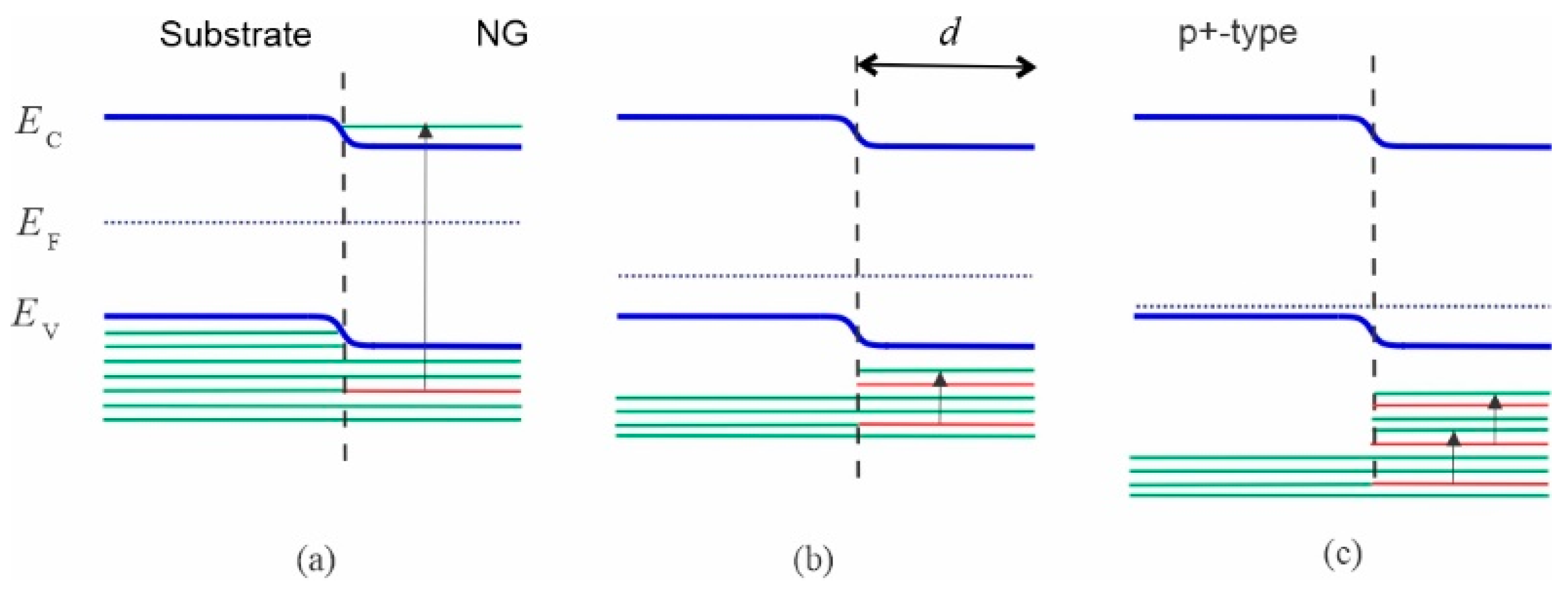
A general energy-band diagram of an intrinsic bulk semiconductor with NG patterns on the surface is shown in Figure 1a. Some of the energy levels in the valence band are forbidden due to reduced quantum states (resulting from NG patterning), and the rejected electrons must occupy the higher energy levels, which in turn, increases the electron concentration in conduction band (G-doping). Figure 1b represents an energy-band diagram of a p-type semiconductor substrate with NG patterns on the surface. In this case, the rejected electrons will, first, move to the top of the valence band and compensate the holes, which raises the Fermi energy level. Figure 1c is the diagram of a p+-type semiconductor with NG patterns on the surface, which only quantitatively differs from that of the p-type semiconductor.
We can state that G-doping is equivalent to donor-doping of the semiconductor as the Fermi energy level of the semiconductor rises under the patterned area. In Figure 1a, an i–n junction forms on the surface of intrinsic substrate with NG patterns. In Figure 1b, (the p-type substrate), depending on G-doping level, a partly compensated p-p− junction, a fully compensated p-i junction, or even a p-n junction can form by tuning the geometry of the NG pattern. In the case of p+-type substrate (Figure 1c), a p+-p junction can be formed. It should be noted that the rejected electrons are confined within the NG layer. Charge neutrality in close proximity of the patterned region does not allow deeper penetration of charges into the substrate and binds the carriers to the characteristic depth d as shown in Figure 1.
In our previous works we fabricated NG layers in bulk p-Si to form a G-doped p-p(v) junction [23]. Analysis of the experimental results has revealed that the G-doping level can be adjusted electrically [24]. Here, we report on the fabrication of G-doped metal-semiconductor junction in p-type and p+-type substrates.
Metal-semiconductor junctions are majority carrier devices allowing very high-frequency operation. Low barrier height and thermionic emission mechanism result in low forward voltages. However, reverse currents are high because of the same reasons and limit applications to DC and microwave electronics. Reverse currents can be reduced by G-doping which will allow wider application of Schottky diodes. G-doping can be used for p-n junctions as well. G-doping allows high carrier mobility, which will improve characteristics of diodes and transistors used in power electronics. Unique optical properties of G-doped layers can be used to improve solar cells and other optoelectronic devices.
2. Sample Preparation and Characterization
Two types of Si substrates, p-type and p+-type, were used for sample preparation. The p-type substrate has a resistivity of 1–10 Ω × cm corresponding to hole concentration p ≈ 3 × 1015 cm−3. The p+-type substrate’s resistivity is 0.044 Ω × cm corresponding to p = 5 × 1017 cm−3 [25] p.32. Samples were cut in 20 mm × 10 mm × 0.5 mm chips. Figure 2 shows the cross-section of the samples. Distance between the nanograting junction and the reference plain junction is 10 mm. Details of the junction’s cross-section are given in Figure 2 of Ref. [23]. Nanograting on the left side induces a G-doped area in close proximity, which forms a p-p (v) junction in the depth (d) of the substrate. Metal-semiconductor contacts were made using Ti metal. Similar contacts on the plain area (right side of the chip, Figure 2) were made during the same manufacturing processes to record the reference I–V characteristics. Comparison of the I–V characteristics recorded from both NG area and reference plain area provides valuable data to observe unique changes in conductivity of patterned surfaces.
NG patterns with a depth of 30 nm and a period of 150 nm were introduced on the surface of silicon substrates using laser interference lithography and subsequent reactive ion etching as described in Ref. [6]. A negative photoresist layer was used for interference lithography to ensure uniform etching of the whole chip’s surface and the indents [22]. This was performed to exclude the influence of reactive ion etching through comparison with the reference area. Both Ti (50 nm thick) and Ag (1000 nm thick) films were grown using DC magnetron sputtering during the single vacuum process. Later, metal contacts were backed at a substrate temperature of 250 °C for 5 min. Back ohmic contacts were made using Al metal and standard metallization process. All contacts were shaped using photolithography and lift-off processes.
Figure 3a shows metal contact layout and wiring both for two-wire and four-wire measurement methods. There are two windows opened in SiO2 contact under layer. Nanograting is fabricated inside the left window only. The right window contains plain Si substrate.
The I–V characteristics were recorded using two-probe and four-probe methods. The two-probe method was used to characterize p-p(v)-M junction. The four-probe method was used to exclude the contribution of metal-semiconductor interface and to record the I–V curve of the pure p-p(v) junction. The voltage and current terminals of I–V measurements are shown in Figure 2. A Keysight multimeter 34410 (input impedance >1 GΩ) and E3640 current source and homemade LabVIEW drivers were used to record I–V curves.
3. Results and Discussion
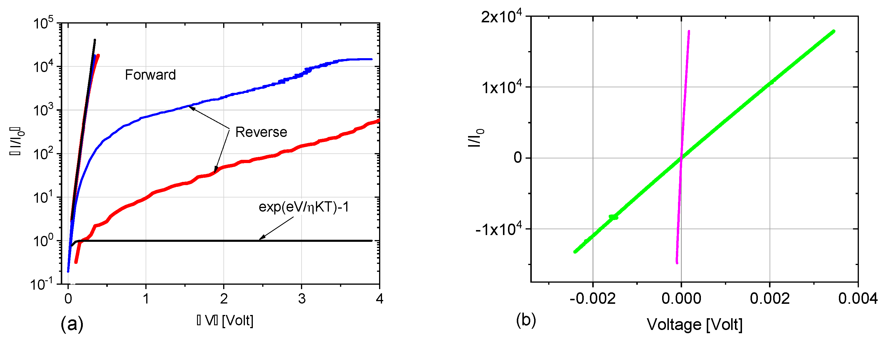
Figure 4a shows the I–V curves of p-p(v)-M and the corresponding reference p-M junction recorded using the two-probe method. Figure 4b shows the I–V curves of the same junctions recorded using the four-probe method which allows excluding the metal-semiconductor interface contribution to the I–V measurements. The curve’s colors correspond to the colors of I− and V-terminal labels of Figure 2. Curves recorded on the NG area are shown in red and green colors. Reference I–V curves shown in blue and violet colors were obtained from analogous measurements made on the reference plain side of the same chip (right side of Figure 2). Comparison of the two pairs of curves (red vs. blue and green vs. violet) allows the identification of the influence of NG patterning on I–V characteristics (forward and reverse currents) separately for two-probe and four-probe measurements, respectively.
As shown in Figure 4a, the forward current () of the p-p(v)-M junction has not been affected by NG patterns. The forward currents of both NG and reference plain junction fit with the Shockley expression with ideality factor of η = 1.25. The reverse current () of the p-p(v)-M junction (Figure 4a) is affected by NG and is considerably lower than the reference p-M junction. The reduction of cannot be explained by the limiting effect of the p-p(v) junction, which is connected in series. This is evident from the reverse current-voltage dependence of the p-p(v) junction (Figure 4b, green curve). Reverse current of p-p(v) junction is considerably higher than that of the p-p(v)-M junction, which can be seen by comparing Figure 4a (red curves) and Figure 4b (green curves). Note the difference in x-axis scales. The reverse current-voltage dependence is stronger for the p-p(v) junction.
To explain the reduction of we repeated the same experiment on p+-type substrate. Figure 5a shows the I–V curves of p+-p(v)-M and the corresponding reference p-M junction measured using the two-probe method. Figure 5b shows the I–V curves of the same junctions recorded using the four-probe method. The curve’s colors correspond to the colors of voltage and current terminals shown in Figure 2.
Forward current of p+-p(v)-M junction (Figure 5a) is not affected by the NG. Forward currents of p+-p(v)-M junction and corresponding reference junction fit well with the Shockley expression, with close ideality factor values (η = 1.25). Current-voltage dependence of p+-p(v) junction (green curve in Figure 5b) indicates that p+-p(v) junction is ohmic type with a resistance higher than the substrate resistance (violet curve in Figure 5b). However, p+-p(v) junction has much lower resistance with respect to the reverse biased p+-p(v)-M junction (see voltage scales in Figure 5a,b). Reverse currents of p+-p(v)-M junction (red curve) are dramatically lower with respect to reference junction. Reduction is as large as 1–2 orders of magnitude in the wide range of reverse voltages (Figure 5a). Reverse current reduction is much more pronounced for the p+-p(v)-M junction with respect to p-p(v)-M junction (Figure 4a). Consequently, the drop in strongly depends on carrier concentration of the substrate.
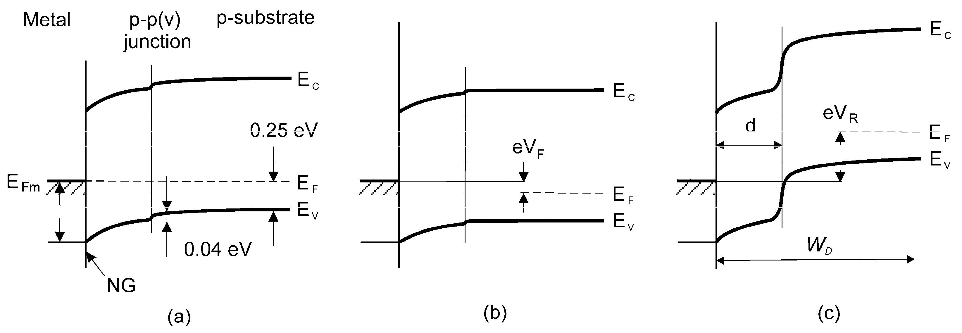
To explain the dependence on carrier concentration, we analyze the relationship between G-doping depth d and the depletion width. The d value does not depend on hole concentration as estimated in Ref. [24] for d ≈ 240 nm. However, the depletion width is 500 nm in p-type substrate and 40 nm in p+-type (calculated for = 1 V) [25] p. 89. Consequently, we have realized two diverse cases in our experiments. In the first case, and in the second case, (p+-type). Let us begin from the p-type substrate: the energy-band diagrams of p-p(v)-M junction is given in Figure 6 and displays the thermal equilibrium (V = 0), forward bias (V > 0), and reverse bias (V < 0) regimes.
The p-p(v) junction falls within the depletion region as shown in Figure 6a. Built-in potential value 0.04 eV is taken from experimental data [23]. Fermi energy is calculated from the hole concentration of the substrate, and the metal-semiconductor barrier is taken for Ti on Si [25] p. 179. In the forward biased regime in Figure 6b, the voltage drop across the p-p(v) junction is much lower than in the metal-semiconductor junction. This follows from the comparison of forward voltage values from Figure 4a. It is also confirmed by a large difference in ideality factors (η = 1.25 for p-p(v)-M junction and η = 0.18 for p-p(v) junction). The voltage distribution is different in the reverse bias regime (Figure 6c). The drop in reverse voltage across p-p(v) junction and metal-semiconductor are comparable, which is confirmed by comparison of reverse voltages in Figure 4a,b (red and green curves). This result is consistent with our previous measurements [23]. Figure 6c indicates that only a part of the depletion region falls within the G-doping region. Consequently, NG-induced changes in semiconductor material properties apply only to a part of the depletion region.
Next, we analyze results obtained from the p+-type substrate. Energy-band diagrams of p+-p(v)-M junction are given in Figure 7. In the forward bias regime, voltage drop across the p-p(v) junction is much lower than in the metal-semiconductor junction. This follows from a comparison of forward voltage values from Figure 5a. The same is true for the reverse bias regime. The I–V characteristics of p+-p(v) is ohmic which is explained by the high hole concentration. Generally, the voltage drop over the p+-p(v) junction is negligible both in forward and reverse bias regimes. The energy-band diagrams in Figure 7 reflect the voltage drop at these junctions. Figure 7c indicates that the whole depletion region falls within the G-doping region. Consequently, NG-induced changes in the material properties of the semiconductor substrates apply to the whole depletion region. Knowing this, we offer the following interpretation for the drop in The DOS reduces in the G-doped layer and this increases the carrier generation lifetime. Consequently, the carrier generation current decreases as it is correspondingly related to lifetime [25] p. 97,
where is an intrinsic carrier concentration and is a carrier generation lifetime. In Equation (1) we ignore the recombination current component as it is negligible in the case of Si (low value) and especially in the case of G-doping, which reduces even more [25]. In the case of G-doped semiconductor, the intrinsic carrier concentration is given by,
where G is the geometry factor [26]. An increase in carrier generation lifetime is a consequence of a general principle called “Fermi’s golden rule” which states that all transition rates are proportional to DOS. Inserting Equation (2) into Equation (1) we obtain,
Equation (3) explains that the generation current is reduced -fold within the G-doped area with respect to the conventionally doped areas. Estimated value for geometry factor is G = 3.3 as presented in Ref. [24]. Consequently, about one order of magnitude reduction in generation current is expected. This explains our results for the drop in in the case of p-type substrate Figure 4a. It should be noted here that the reverse currents should be compared for the same value (for the same VR). Consequently, p-p(v) junction voltage drop is considerable and should be determined from Figure 4b (for the same current) and subtracted from the x-axis of Figure 4a before applying to the green curve. After this procedure, reverse current reduction (Figure 4a) increases to roughly one order of magnitude and is in good agreement with Equation (3). In the case of a p-type substrate, the depletion region is relatively wide and includes a G-doped region (Figure 6c). Consequently, the generation current reduces at a small part of the depletion region. In case of p+-type substrate, the depletion region shrinks dramatically and becomes a part of the G-doping region itself (Figure 7c). Here, the generation current is reduced within the whole depletion region. This can explain why reduction is more pronounced in p+-type substrates. The Si-based G-doped Schottky diodes I–V curves are comparable to I–V curves obtained on the basis of more advanced materials (AlN and GaN) [27]. Further improvement of G-doping-based junctions can be made by tuning the Fermi level using nanograting depth variation [22]. We plan to tune the Fermi level by varying the NG line width as well.
Reduced reverse currents in G-doped junctions can be used to significantly increase the quality of metal-semiconductor diodes by eliminating their main drawback—relatively high reverse currents. We estimated G-doping depth as d ≈ 240 nm in Ref. [24] and used this value to explain the concept through energy-band diagrams. This value fits well between = 40 nm for p+-type and = 500 nm for a p-type substrate. However, the direct measurement of d is essential. We are planning the direct measurements of G-doping depth and its voltage dependence in our future experiments.
4. Conclusions
We have fabricated and characterized G-doping-based metal-semiconductor junctions. The p-type and p+-type silicon substrates were used as semiconductor material and Ti as metallic electrode. To realize G-doping, nanograting was patterned on the surface of Si substrates. It was found that forward current-voltage dependence of p-p(v)-M and p+-p(v)-M junctions are well described by the Shockley equation. The reverse current of p-p(v)-M junction is considerably lower with respect to the p-M junction. Reverse current of p+-p(v)-M junction is reduced even more and is 1–2 orders of magnitude less with respect to the p+-M junction. Experimental results are in agreement with the G-doping theory and the p-p(v) junction formation mechanism developed earlier. Low reverse currents are explained by the reduction of carrier generation current within the depletion region, which itself is a consequence of reduced DOS within the G-doped region. Substrate carrier concentration dependence is analyzed using energy-band diagrams. In the case of a p-type substrate, the depletion region includes the G-doped region. In the case of p+-type substrate, the depletion region shrinks dramatically and becomes a part of the G-doping region itself. Reduced reverse currents can be employed to significantly increase the quality of metal-semiconductor diodes widely used in high-frequency and general electronics.
Author Contributions
A.T.: writing—original draft, methodology, experimental research, funding acquisition; L.J.: methodology, experimental research; Z.T.: experimental research; N.E.G.: manuscript review, funding acquisition. All authors have read and agreed to the published version of the manuscript.
Funding
Research was funded by Shota Rustaveli National Science Foundation (SRNSF) and Georgia National Innovation Ecosystem, grant number CARYS-19-218.
Institutional Review Board Statement
Not applicable.
Informed Consent Statement
Not applicable.
Data Availability Statement
Data sharing not applicable.
Acknowledgments
The authors would like to thank G. Skhiladze, S. Sikharulidze, and N. Kitoshvili for supporting the project.
Conflicts of Interest
The authors declare no conflict of interest.
References
- Mukherjee, P.; Bruccoleri, A.; Heilmann, R.K.; Schattenburg, M.L.; Kaplan, A.F.; Guo, L.J. Plasma etch fabrication of 60:1 aspect ratio silicon nanogratings with 200 nm pitch. J. Vac. Sci. Technol. B 2010, 28, C6P70–C6P75. [Google Scholar] [CrossRef]
- Li, H.; Wang, X.; Zhu, X.; Duan, X.; Pan, A. Composition modulation in one-dimensional and two-dimensional chalcogenide semiconductor nanostructures. Chem. Soc. Rev. 2018, 47, 7504. [Google Scholar] [CrossRef]
- Miyazaki, K.; Miyaji, G.; Inoue, T. Nanograting formation on metals in air with interfering femtosecond laser pulses. Appl. Phys. Lett. 2015, 107, 071103. [Google Scholar] [CrossRef] [Green Version]
- Jia, T.; Wang, X.; Ren, Y.; Su, Y.; Zhang, L.; Yang, H.; Zhang, L.; Liu, W. Incidence angle effects on the fabrication of microstructures using six-beam laser interference lithography. Coatings 2021, 11, 62. [Google Scholar] [CrossRef]
- Tavkhelidze, A. Geometry-induced electron doping in periodic semiconductor nanostructures. Phys. E 2014, 60, 4. [Google Scholar] [CrossRef] [Green Version]
- Tavkhelidze, A.; Jangidze, L.; Mebonia, M.; Piotrowski, K.; Więckowski, J.; Taliashvili, Z.; Skhiladze, G.; Nadaraia, L. Geometry--induced quantum effects in periodic nanostructures. Phys. Staus. Solidi. A 2017, 214, 1700334. [Google Scholar] [CrossRef]
- Samoila, C.; Ursutiu, D.; Tavkhelidze, A.; Jangidze, L.; Taliashvili, Z.; Skhiladze, G.; Tierean, M.H. Nanograting layers of Si. Nanotechnology 2020, 31, 035301. [Google Scholar] [CrossRef] [PubMed]
- Tavkhelidze, A.; Grabecki, G.; Jangidze, L.; Yahniuk, I.; Taliashvili, Z.; Taliashvili, B. Negative Magnetoresistance in Si Nanograting Layers. Phys. Status Solidi A 2019, 216, 1800693. [Google Scholar] [CrossRef]
- Gu, H.; Zhang, H.; Lin, J.; Shao, Q.; Young, D.P.; Sun, L.; Shen, T.D.; Guo, Z. Large negative giant magnetoresistance at room temperature and electrical transport in cobalt ferrite-polyaniline nanocomposites. Polymer 2018, 143, 324–330. [Google Scholar] [CrossRef]
- Bayramov, A.; Alizade, E.; Mammadov, S.; Tavkhelidze, A.; Mamedov, N.; Aliyeva, Y.; Ahmedova, K.; Asadullayeva, S.; Jangidze, L.; Skhiladze, G. Optical properties of surface grated SI–based multilayer structure. J. Vac. Sci. Technol. B 2019, 37, 061807. [Google Scholar] [CrossRef]
- Nie, M.; Zhao, Y.; Zeng, Y. Effects of annealing and laser irradiation on optical and electrical properties of ZnO thin films. J. Laser Appl. 2014, 26, 022005. [Google Scholar] [CrossRef]
- Luo, L.-B.; Xie, C.; Wang, X.-H.; Yu, Y.-Q.; Wu, C.-Y.; Hu, H.; Zhou, K.-Y.; Zhang, X.-W.; Jie, J.-S. Surface plasmon resonance enhanced highly efficient planar silicon solar cell. Nano Energy 2014, 9, 112–120. [Google Scholar] [CrossRef]
- Mamedov, N.; Tavkhelidze, A.; Bayramov, A.; Akhmedova, K.; Aliyeva, Y.; Eyyubov, G.; Jangidze, L.; Skhiladze, G. Spectroscopic planar diffraction ellipsometry of SI–based multilayer structure with subwavelength grating. Phys. Status Solidi C 2017, 1700092. [Google Scholar] [CrossRef]
- Tavkhelidze, A.; Bayramov, A.; Aliyeva, Y.; Jangidze, L.; Skhiladze, G.; Asadullayeva, S.; Alekperov, O.; Mamedov, N. Optical and electronic properties of periodic Si nanostructures. Phys. Status Solidi C 2017, 14, 1700093. [Google Scholar] [CrossRef]
- Evtukh, A.; Medvid, A.; Onufrijevs, P.; Okada, M.; Mimura, H. Electron field emission from the Si nanostructures formed by laser irradiation. J. Vac. Sci. Technol. B 2010, 28, C2B11. [Google Scholar] [CrossRef]
- Tavkhelidze, A.; Bibilashvili, A.; Jangidze, L.; Shimkunas, A.; Mauger, P.; Rempfer, G.F.; Almaraz, L.; Dixon, T.; Kordesch, M.E.; Katan, N.; et al. Observation of quantum interference effect in solids. J. Vac. Sci. Technol. B 2006, 24, 1413. [Google Scholar] [CrossRef] [Green Version]
- Kakulia, D.; Tavkhelidze, A.; Gogoberidze, V.; Mebonia, M. Density of quantum states in quasI–1D layers. Phys. E 2016, 78, 49. [Google Scholar] [CrossRef] [Green Version]
- Luchenko, A.I.; Melnichenko, N.; Svezhentsova, K.V. Local Electronic Properties of the Surface of the Nanostructured Silicon Layers. In Proceedings of the 2016 IEEE 36th International Conference on Electronics and Nanotechnology (ELNANO), Kyiv, Ukraine, 19–21 April 2016; p. 43. [Google Scholar]
- Medvid, A.; Onufrijevs, P.; Jarimaviciute-Gudaitiene, R.; Dauksta, E.; Prosycevas, I. Formation mechanisms of nano and microcones by laser radiation on surfaces of Si, Ge, and SiGe crystals. Nanoscale Res. Lett. 2013, 8, 264. [Google Scholar] [CrossRef] [Green Version]
- Medvid, A.; Onufrievs, P.; Dauksta, E.; Barloti, J.; Ulyashin, A.; Dmytruk, I.; Pundyk, I. P-N Junction formation in ITO/p-Si structure by powerful laser radiation for solar cells applications. Adv. Mater. Res. 2011, 222, 225–228. [Google Scholar] [CrossRef]
- Mortazavi, S.; Mollabashi, M.; Barri, R.; Gundlach, L.; Jones, K.; Xiao, J.Q.; Oplia, R.L.; Shah, S.I. Ti: Sapphire laser irradiation of graphene oxide film in order to tune its structural, chemical and electrical properties: Patterning and characterizations. Appl. Surf. Sci. 2020, 500, 144053. [Google Scholar] [CrossRef]
- Tavkhelidze, A.; Bibilashvili, A.; Jangidze, L.; Gorji, N.E. FermI–level tuning of G-doped layers. Nanomaterials 2021, 11, 505. [Google Scholar] [CrossRef]
- Tavkhelidze, A.; Jangidze, L.; Skhiladze, G. G-doping based nanostructured p-p(v) junction. Mater. Res. Express 2019, 6, 075049. [Google Scholar] [CrossRef] [Green Version]
- Tavkhelidze, A. G-doping junction-formation mechanism. Semicond. Sci. Technol. 2020, 35, 075005. [Google Scholar] [CrossRef]
- Sze, S.M.; Ng, K.K. Physics of Semiconductor Devices; Wiley Interscience: Hoboken, NJ, USA, 2007. [Google Scholar]
- Tavkhelidze, A. Large enhancement of the thermoelectric figure of merit in a ridged quantum well. Nanotechnology 2009, 20, 405401. [Google Scholar] [CrossRef] [PubMed]
- Kim, H.; Choi, S.; Choi, B.J. Influence of AlN and GaN Pulse ratios in thermal atomic layer deposited AlGaN on the electrical properties of AlGaN/GaN schottky diodes. Coatings 2020, 10, 489. [Google Scholar] [CrossRef]
Figure 1.
Basic energy-band diagrams of NG layers fabricated on the surface of (a) an intrinsic semiconductor, (b) a p-type, and (c) a p+-type. The green lines refer to energy levels occupied by electrons, and red lines refer to energy levels forbidden by NG patterns.
Figure 1.
Basic energy-band diagrams of NG layers fabricated on the surface of (a) an intrinsic semiconductor, (b) a p-type, and (c) a p+-type. The green lines refer to energy levels occupied by electrons, and red lines refer to energy levels forbidden by NG patterns.

Figure 2.
Cross-section of the prepared sample: (a) representing p-p(v)-M junction and (b) representing reference junction. The I- and V- labels represent the location of the 2-probe and 4-probe measurements.
Figure 2.
Cross-section of the prepared sample: (a) representing p-p(v)-M junction and (b) representing reference junction. The I- and V- labels represent the location of the 2-probe and 4-probe measurements.

Figure 3.
(a) Front side metal contact layout. Nanograting is fabricated inside the window opened in SiO2 layer. (b) Back side contact layout.
Figure 3.
(a) Front side metal contact layout. Nanograting is fabricated inside the window opened in SiO2 layer. (b) Back side contact layout.

Figure 4.
The I–V curves of p-type sample: (a) two-probe; (b) four-probe measurements. The red color corresponds to the nanograting area recorded using two probes; the blue color refers to the I–V recorded from the plain area using two probes; the green color refers to the nanograting area recorded using four probes, and the violet refers to the plain area recorded using four probes. Colors correspond to voltage and current terminals shown in Figure 2. Shockley equation fitting curve (for η = 1.25) is shown in black.

Figure 5.
The I–V curves of p+-type sample: (a) two-probe; (b) four-probe. The red color corresponds to the nanograting area recorded using two probes; the blue refers to the plain area recorded using two probes; the green color refers to the nanograting area recorded using four probes; and the violet refers to the plain area recorded using four probes. Colors correspond to voltage and current terminals labels in Figure 2. Shockley equation fitting curve (for η = 1.25) is shown in black color.

Figure 6.
Energy-band diagram of p-p(v)-M junction: (a) thermal equilibrium; (b) forward bias; (c) reverse bias. Distances and energies (except the eVR) are scaled according to their experimental values.
Figure 6.
Energy-band diagram of p-p(v)-M junction: (a) thermal equilibrium; (b) forward bias; (c) reverse bias. Distances and energies (except the eVR) are scaled according to their experimental values.

Figure 7.
Energy-band diagram for p-p(v)-M junction. (a) Thermal equilibrium; (b) forward bias; (c) reverse bias. Distances and energies (except eVR) are scaled according to their experimental values.
Figure 7.
Energy-band diagram for p-p(v)-M junction. (a) Thermal equilibrium; (b) forward bias; (c) reverse bias. Distances and energies (except eVR) are scaled according to their experimental values.

Publisher’s Note: MDPI stays neutral with regard to jurisdictional claims in published maps and institutional affiliations. |
© 2021 by the authors. Licensee MDPI, Basel, Switzerland. This article is an open access article distributed under the terms and conditions of the Creative Commons Attribution (CC BY) license (https://creativecommons.org/licenses/by/4.0/).
Share and Cite
MDPI and ACS Style
Tavkhelidze, A.; Jangidze, L.; Taliashvili, Z.; Gorji, N.E. G-Doping-Based Metal-Semiconductor Junction. Coatings 2021, 11, 945. https://doi.org/10.3390/coatings11080945
AMA Style
Tavkhelidze A, Jangidze L, Taliashvili Z, Gorji NE. G-Doping-Based Metal-Semiconductor Junction. Coatings. 2021; 11(8):945. https://doi.org/10.3390/coatings11080945
Chicago/Turabian StyleTavkhelidze, Avtandil, Larissa Jangidze, Zaza Taliashvili, and Nima E. Gorji. 2021. "G-Doping-Based Metal-Semiconductor Junction" Coatings 11, no. 8: 945. https://doi.org/10.3390/coatings11080945
Note that from the first issue of 2016, this journal uses article numbers instead of page numbers. See further details here.