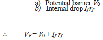
- It is generally profitable to replace a device or system by its equivalent circuit. An equivalent circuit of a device (e.g. crystal diode, transistor etc.) is a combination of electric elements, which when connected in a circuit, acts exactly as does the device when connected in the same circuit. Once the device is replaced by its equivalent circuit, the resulting network can be solved by traditional circuit analysis techniques. We shall now find the equivalent circuit of a crystal diode.
(i) Approximate Equivalent circuit: When the forward voltage V
F is applied across a diode, it will not conduct till the potential barrier V
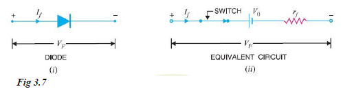
0 at the junction is overcome. When the forward voltage exceeds the potential barrier voltage, the diode starts conducting as shown in Fig. 3.7 (i). The forward current I
f flowing through the diode causes a voltage drop in its internal resistance r
f. Therefore, the forward voltage V
F applied across the actual diode has to overcome:
- For a silicon diode, V
0 = 0.7 V whereas for a germanium diode, V
0 = 0.3 V.
Therefore, approximate equivalent circuit for a crystal diode is a switch in series with a battery V
0 and internal resistance r
f as shown in Fig. 3.7 (ii). This approximate equivalent circuit of a diode is very helpful in studying the performance of the diode in a circuit.
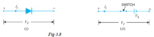
 (ii) ) Simplified Equivalent circuit:
 For most applications, the internal resistance r
f of the crystal diode can be ignored in comparison to other elements in the equivalent circuit. The equivalent circuit then reduces to the one shown in Fig. 3.8 (ii). This simplified equivalent circuit of the crystal diode is frequently used in diode-circuit analysis.
- Forward biased and as a perfect insulator when reverse biased. Obviously, in such a hypothetical situation, forward resistance r
f = 0 and potential barrier V
0 is considered negligible. It may be mentioned here that although ideal diode is never found in practice, yet diode circuit analysis is made on this basis. Therefore, while discussing diode circuits, the diode will be assumed ideal unless and until stated otherwise.
Wilfykil answered the question on
August 14, 2019 at 07:06