Historical Perspectives, State of art and Research Trends of Single Photon Avalanche Diodes and Their Applications (Part 1: Single Pixels)
 Iris Cusini*
  Davide Berretta Enrico Conca Alfonso Incoronato
  Francesca Madonini Arianna Adelaide Maurina Chiara Nonne Simone Riccardo
  Federica Villa
- Dipartimento di Elettronica, Informazione e Bioingegneria, Politecnico di Milano, Milano, Italy
The ability to detect single photons is becoming an enabling key capability in an increasing number of fields. Indeed, its scope is not limited to applications that specifically rely on single photons, such as quantum imaging, but extends to applications where a low signal is overwhelmed by background light, such as laser ranging, or in which faint excitation light is required not to damage the sample or harm the patient. In the last decades, SPADs gained popularity with respect to other single-photon detectors thanks to their small size, possibility to be integrated in Complementary Metal-Oxide Semiconductor processes, room temperature operability, low power supply and, above all, the possibility to be fast gated (to time filter the incoming signal) and to precisely timestamp the detected photons. The development of large digital arrays that integrates the detectors and circuits has allowed the implementation of complex functionality on-chip, tailoring the detectors to suit the need of specific applications. This review proposes a complete overview of silicon SPADs characteristics and applications. In this Part I, starting with the working principle, simulation models and required frontend, the paper moves to the most common parameters adopted in literature for characterizing SPADs, and describes single pixels applications and their performance. In the next Part II, the focus is then posed on the development of SPAD arrays, presenting some of the most notable examples found in literature. The actual exploitation of these designs in real applications (e.g., automotive, bioimaging and radiation detectors) is then discussed.
1 Introduction
Through the years, solid-state and especially single-photon imaging techniques have benefited from silicon electro-optical properties and integrability potential. In fact, a wide range of semiconductor optical detectors has been studied and employed.
Among such a variety of options, photodiodes figure as the simplest and cheapest ones [1]. To convert an incident radiation into an electrical signal, the diode is reverse biased and thus depleted from free carriers. When a photon is absorbed in the material, it transfers to the structure the energy necessary to generate an electron-hole pair, which is then collected by the readout circuit. However, when operating in photon-starving conditions proper to many fields of interest, such devices show a critical signal-to-noise ratio mainly because of the readout electronics noise. Therefore, an internal gain multiplication is mandatory.
In Avalanche Photodiodes (APDs), being biased slightly below the breakdown voltage, photogenerated carriers undergo an impact ionization process, generating avalanche multiplication and a finite gain [2]. APDs operate in linear/analog mode and the maximum useful gain is limited by strong fluctuations in the multiplication procedure. Thus, they are unsuitable for time-correlated imaging techniques, where it may be required single-photon sensitivity and an effective time-gating of the detector operation.
Instead, single photons can be detected by APDs operated above the breakdown voltage (Geiger mode) [3]. Such sensors are known as Single Photon Avalanche Diodes (SPADs). When a photon is absorbed in the multiplication region of the device, a self-sustaining avalanche may be triggered and the current increases rapidly to a well-detectable level, marking with picoseconds time resolution the arrival time of the detected photon. An external circuit is then needed to quench the multiplication process and restore the SPAD to its original state, preparing it to detect a new photon [4]. The main drawback of SPADs with respect to analog detectors is the presence of a deadtime after each photon detection which limits the maximum count rate. To bring together the advantages of single-photon detection, typical of SPADs, and the photon number resolution, typical of analog detectors, solid-state photodetectors made of many SPADs connected in parallel, i.e., Silicon Photomultipliers (SiPMs), are widely exploited. The possibility to count each triggered avalanche is achievable both in an analog fashion (aSiPM), where each microcell employs a resistor for passive quenching of the SPAD, and in digital SiPM (dSiPM), integrating every SPAD with its own active or passive quenching and readout circuit [5].
Notwithstanding many single-photon sensitive devices already existed, SPADs stick out because of some advantages over the most promising one, e.g., Photomultiplier Tubes (PMTs) and Superconductive Nanowire Single-Photon Detectors (SNSPDs). Indeed, PMTs require high bias voltages, are bulky and sensitive to magnetic fields, and cannot be integrated with Complementary Metal-Oxide Semiconductor (CMOS) electronics, while SNSPDs require a cryostat to cool down the detector to a few Kelvins, making the system bulky and consequently limiting the application fields [6].
Arrays of SPADs are eligible for high-sensitivity imaging, superseding Charge-Coupled Devices (CCDs) and CMOS Active Pixel Sensors (APSs) when high-frame rates, gating, and photon timing capabilities are required. In fact, CCDs charge transfer readout results in a limited frame rate, whereas CMOS APSs, albeit being fast, do not detect faint signals, because they do not use internal amplification. More expensive Intensified-CCDs (I-CCDs) and Electron-Multiplying-CCDs (EMCCDs), having an internal gain, are employed to increase the signal [7, 8]; however, they cannot provide frame rates higher than few kframe/s and cannot be used in precise time resolved measurements. Eventually, arrays of SPADs and SiPMs are employed to overcome such tradeoffs.
From a historical perspective, single-photon detection by means of p-n junctions was first proposed by Haitz in Shockley Laboratory in the early 1960s [9, 10]. With the studies on the micro-plasma instabilities in silicon, he pioneered the understanding of avalanche breakdown and dark-current pulses, successfully modeling the first diode operating in Geiger mode. However, the evolution toward efficient Single Photon Detectors (SPDs) stepped forward with the development of the first epitaxial devices in the late 1980s [11], achieving good control of the electric field in the active region and thus its influence on dark counts, afterpulsing probability, and temperature dependence. Another milestone in the usage of SPADs was represented by the introduction of Active Quenching Circuits (AQCs), developed in 1981 by Cova [12]. By sensing the rise of the avalanche pulse and reacting back on the SPAD, these architectures force the quenching and reset transitions in short times (few nanoseconds) with a controlled bias-voltage source, paving the way for Single-Photon Counting (SPC) and Time-Correlated Single-Photon Counting (TCSPC) applications. A decade later, with ICs technology nodes miniaturization, custom fabricated SPADs combined with compact active frontend were developed [13]. Fully dedicated and flexible fabrication provided best-in-class performance in terms of detection efficiency, noise, and jitter. However, the impossibility of monolithic integration with processing electronics confined their application only in single- or some- (up to about one hundred) pixel arrays. Later on, thousands of SPADs have been assembled in arrays of a few millimeters square using the technological solution proposed firstly by Golovin [14]. The rising request for integrated circuits for control electronics in the 90s and early 2000s, set technological constraints fairly consistent with those set by SPADs, leading to the fabrication of on-chip integrated sensors in standard CMOS technology. Among the first attempts, in 2003 single pixel CMOS SPADs [15] and then fully integrated 2D arrays have been developed by A. Rochas et al. [16]. This allowed monolithic integration on the same silicon wafer of photodetectors, analog avalanche sensing and quenching, and digital electronics for SPC and TCSPC. In the last few decades, more advanced technologies such as 3D-stacking [17] have gained ground. Such architecture overlaps the sensor tier to the processing electronic, thus enabling independent optimization of each layer with dedicated processes, promising better sensitivity and more functionalities per pixel. Aull was the first to investigate 3D-stacked SPAD arrays in 2006 [18], while a decade later Mata Pavia [19] firstly demonstrated back-illuminated 3D-stacked SPAD image sensors based on standard CMOS technology.
SPADs stand out for their digital output, single-photon sensitivity, fast-gated operation, and picosecond precision, while remaining compact, low cost, and easy-to-integrate. Hence, they have been applied at first when intensity and time-dependent waveform of faint optical signals needed to be reconstructed. Beginning with academic research purposes in astrophysics [20], Adaptive Optics [21] and Fluorescent Imaging [22], during the years, the implementation on-chip of smart SPC and TCSPC increased the commercial and industrial appeal of such detectors, raising the interest of many big players (e.g., STMicroelctronics, Toyota, Sony, Samsung, Apple) in mobile/consumer electronics. Nowadays, several fields of applications are covered, spanning from biophotonics [23], Light Detection and Ranging (LiDAR) [24] and 3-D optical ranging applications [25], to quantum information technologies [26, 27].
Furthermore, arrays of SPADs and SiPMs tend to replace traditional PMTs in many radiation detection applications [28]. Large aSiPMs are already an established reality in indirect detection of gamma rays for Positron Emission Tomography (PET), offering a high fill-factor (FF), fast collection of highly energetic photons, and magnetic fields immunity [29]. However, dSiPMs are gaining more and more interest in Time-Of-Flight (TOF) PET, promising an improved coincidence time resolution, increased timestamp granularity and direct on-chip processing. Usage of 3D-stacked SPADs as detectors in X-rays radiation environments has also been recently documented [30].
The aim of this article is to review the main features of silicon SPADs and their figures of merit. Section 2 covers the description of SPADs physics. Section 3 is dedicated to the different frontend architectures, Section 4 focuses on the main SPAD figures of merit while Section 5 presents single pixels applications and their performance.
2 SPAD Detector
2.1 SPAD Working Principle
SPADs consist of a p-n junction biased above the breakdown voltage (VB) and are characterized by an intrinsic positive feedback, which is the fundamental mechanism behind their single-photon sensitivity. This condition happens when the electric field is so high to reach a critical value (>3.105 V/cm) due to the applied reverse bias across the p-n junction, overcoming the VB with an overvoltage named excess bias (VEX). In fact, SPADs operate in a bistable condition in which the device is either in a quiescent state or the avalanche is triggered. A SPAD must be able to remain quiescent, when biased above breakdown, for a sufficient amount of time (e.g., longer than ms), waiting for the avalanche current injection. Thus, the spontaneous generation-recombination phenomena, which would trigger the avalanche multiplication process independently of the light signal, must be kept as low as possible. As soon as an electron-hole pair is generated an avalanche current is generated, typically increasing with a rise time below 1 ns up to a steady current level in the mA range. The current converges to a self-sustaining level, as a consequence of a counteracting effect due to the generated free carriers in the depleted region, able to mitigate the electric field. The SPAD outcoming pulse due to a single-photon detection has a sufficient amplitude to be easily detected by a readout electronics; for this reason SPADs are considered SPD [31–34]. The high value of avalanche current in a SPAD risks to stress and damage the junction. Consequently, to stop this current and avoid breaking the device, it is essential to lower the electric field adequately below the critical value (≈3.105 V/cm), effectively quenching the avalanche. Thus, the frontend electronics has the task to detect the leading edge of the avalanche, generate an output pulse synchronous with the triggering, promptly reduce the SPAD bias to the breakdown voltage and finally restore the initial operative level. This circuit is usually referred to as a sensing, quenching and recharge circuit or simply quenching circuit [13]. In the current-voltage (I-V) characteristic, shown in Figure 1, the on-branch represents the sweeps after the avalanche has been triggered and the SPAD is being quenched, the off-branch, instead, the sweeps during the recharge phase.
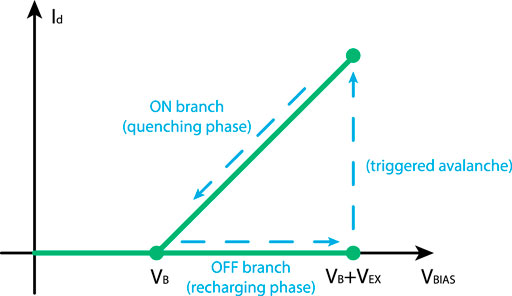
FIGURE 1. SPAD I-V characteristic. The voltage VBIAS is the reverse bias applied to the SPAD and Id the SPAD current.
Quenching circuits are necessary to avoid SPAD damage by promptly interrupting the avalanche current flow through a reduction of the reverse voltage below VB. Various are the proposed solutions for quenching that come with either passive or active components, or a mix of the two, answering to different design requirements (see Section 3).
2.2 Cross-Section in Different Technologies
The technology employed to fabricate the SPAD and the device cross-section, deeply influences the detector performance. SPADs can be fabricated either in Custom technologies or Standard CMOS technologies. A custom fabrication process was employed in the earliest published works on SPAD detectors [35, 36], achieving very good device performance. The main advantage of custom technology is the flexibility to act on dopant concentration and implantation energy, targeting the optimization of SPAD performance. Nevertheless, custom SPADs have high production costs, cannot be integrated with frontend circuitry and their parameters are not homogeneous on different production batches. Thus, this process is mainly employed for single devices or small arrays of the detectors.
Custom SPADs are gathered in two families: reach-through and planar devices. The typical structure of a reach-through SPAD is shown in Figure 2A. Considering a quasi-intrinsic p− substrate, the high electric field region is at the junction created on one side by an n+ phosphorous diffusion, while on the other side by a deeper p+ boron enrichment. By applying an appropriate reverse bias, the depleted region extends into the entire p− layer. This structure reaches high efficiency thanks to the wide depleted region and having the avalanche initiated by electrons (being a p/n+ geometry), however the large area allows the triggering of the avalanche in different regions with a different propagation time of the current, worsening the timing performance. The backside of the wafer is etched targeting a thickness of 25–40 μm. However, reach-through SPADs are not suitable for array implementation, being delicate and costly devices [3]. On the contrary, a planar structure is easier to fabricate [37–39]. A possible example of cross-section can be found in Figure 2B, the junction is relatively shallow, obtained through an n+ phosphorous diffusion and an ion implantation p enrichment. The substrate is one of the main differences with respect to the reach-through SPAD. It is composed of an n+ wafer plus the addition of a quasi-intrinsic p region and a p+ buried one, both through epitaxy. The high doping n+ region introduces a full electrical isolation and sharply reduces the diffusions tails. The planar structure requires a lower bias and assures very good timing response, making it possible to create arrays of detectors (still without frontend electronics). In order to obtain higher efficiency in the Near-Infrared (NIR) range, two different structures of custom planar SPADs have been engineered: red-enhanced [40, 41] and resonant-cavity-enhanced SPADs [42, 43].
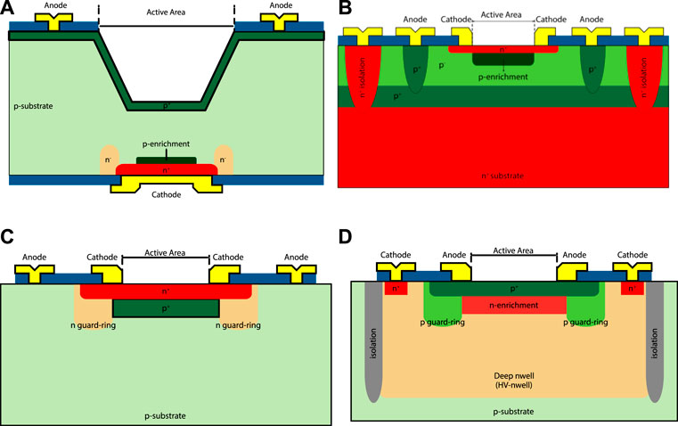
FIGURE 2. SPAD cross-sections: reach-through custom SPAD (A), planar custom SPAD (B), non-isolated CMOS SPAD (C), and isolated CMOS SPAD (D).
Standard CMOS SPADs have clear advantages compared to custom devices. First of all, the possibility to be integrated into silicon wafers, optimizing the area employment with high resolution and low cost per pixel. As a direct outcome, integrated SPADs allow the design of arrays, up to massive size, together with the design of complex frontends, processing and readout. The main drawback of SPAD integration in well-consolidated commercial technologies is the rigidity of processes, since realizing the specific technology masks requires a significant economical effort. However, integrated SPADs have shown a key role in many applications, so they have been introduced alongside the core products of some foundries [44]. CMOS SPADs are divided into non-isolated and isolated devices [45]. The formers have a central cathode surrounded by the anode, which is directly in contact with the substrate (Figure 2C), resulting in a deep depleted region that enhances the NIR sensitivity [46], but worsens the timing performance. Isolated SPADs are typically designed by diffusing a controlled n+ enrichment in the center of the junction, beneath a highly doped shallow p+ boron implantation in an n-doped well (Figure 2D). In the central region, the breakdown voltage is reduced, thus it acts as the active area, compared to the edge abrupt p+n junction that presents a lower electric field. Instead of the enrichment, a doughnut-shaped p− diffusion covering just the edge of the p+ implantation can be used as a “guard-ring” to prevent edge breakdown. The depletion region can be about 0.3–1 µm thick across the active area, depending on the thickness and doping concentration of the n-well. The anode metal layer is laid out not only to contact the top p+ implantation, but also to act as a pin-hole, thus exposing only the active area to the incident light, while shielding all the surrounding regions. The use of isolation techniques helps in protecting the circuit from the cathode high voltage also limiting the electrical crosstalk.
Besides the differences in technology, there are two approaches to illuminate the SPADs: Front-Side Illumination (FSI) and Back-Side Illumination (BSI). An insight is provided in Part II of this paper.
2.3 SPAD Modeling
A consistent model, able to predict the device behavior in all conditions, is fundamental in a solid workflow for designing the frontend circuit. A starting point for the SPAD model structure is the one proposed in [47] which represents a good approximation of the SPAD main operation principles. As illustrated in Figure 3, its schematic includes two parallel branches: the first one composed of the series of the device resistance (RD), the avalanche switch, and the VB voltage generator, while the second one composed of the junction capacitance (CJ). RD is the diode internal resistance given by the sum of the space-charge layer resistance (RSCL) and the ohmic resistance of neutral regions crossed by the avalanche current (RSERIES) [13]. Its value depends on the device structure varying from a few hundred ohms up to some kΩ: the smaller the active area and the wider the undepleted silicon, the higher the resistance gets. The switch emulates the avalanche, getting closed when an avalanche occurs and opened when the avalanche is quenched. CJ is the junction capacitance, which is the capacitance of the depleted region, which varies with the SPAD bias voltage and the selected SPAD geometry, with typical values ranging from fF to pF. In addition, there are two stray capacitances, CANODE and CCATHODE (connected respectively to anode and cathode sides), which take into account parasitisms of the SPAD cross-section. The values of every single parameter of the SPAD model are usually estimated through TCAD simulations or measured on fabricated devices. Even more sophisticated models can be found in the literature, based on Verilog-A language, in which a mimic of statistics and noise is introduced [48–51].
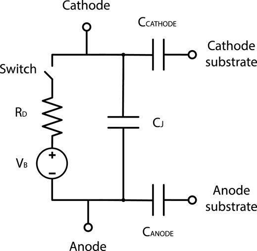
FIGURE 3. SPAD model, which includes the breakdown voltage generator, the detector resistance, the junction capacitance and the anode and cathode parasitic capacitances.
3 SPAD Frontends
3.1 Passive Quenching Circuits
The Passive Quenching Circuit (PQC) consists in a simple resistor (RQ) connected either to the SPAD cathode or anode and often followed by a comparator to provide a digital output (Figure 4A). Basically, after triggering an avalanche, a huge current starts flowing through the resistor, which creates the voltage drop equal to VEX required to bring the SPAD at a bias equal to VB, thus interrupting the avalanche current [13, 52, 53]. It is possible to distinguish two different phases in the PQC operation: quenching and reset transitions. These two phases raise a trade-off on the optimum value of the quenching resistor (RQ), as it will be clarified in the following discussion. During the quenching phase, the depleted capacitance (CJ) is discharged, undergoing a voltage drop equal to VEX, on the other hand the anode or cathode parasitic capacitance is charged with the same amount. A high value of the resistance is suitable for reducing the quenching time after the event detection, promptly producing the appropriate voltage pulse. The avalanche current flowing in the junction (ID) is characterized by an exponential decrease in which the reached peak value is
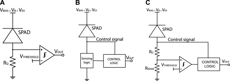
FIGURE 4. Quenching circuits: example of passive quenching circuit (A), block representation of an active quenching circuit (B) and of a Variable Load Quenching Circuit (C).
Typically, RQ is some order of magnitude higher than RD, justifying the approximation done in both expressions.
Considering the avalanche physics, when the voltage across the diode is approaching VB, the impact ionization probability decreases, and consequently also the number of carriers in the depleted region decreases. Being a statistical process, to have a negligible probability of electron-hole pairs creation in the high-field region, the current value should drop below a threshold value, namely Ilatching, usually in the order of 100 μA [13], thus RQ is sized in order to assure an
Thus, a high value of RQ results in a long reset phase, with a related limitation of the maximum count rate. To optimize both the quenching and reset phase, the typical values of RQ range from tens of kΩ to hundreds of kΩ.
An intrinsic drawback of the PQC is the non-controlled hold-off time of the SPAD, in fact during the reset phase another photon can trigger a new event, with different probability depending on the excess voltage across the SPAD, which increases during the reset. These pulses keep the output of the comparator always high, thus causing significant count losses. In integrated solutions, the quenching resistor can be implemented for instance with poly-resistors, or, in order to reduce the area consumption, with transistors working in their ohmic region, even though they introduce some limitations in terms of maximum VEX.
3.2 Active Quenching Circuits
To overcome PQC limitations, the Active Quenching Circuit (AQC) has been proposed, the first one is described in [31]. The avalanche sensing, the quenching and the recharge phases rely on active components (Figure 4B), not suffering from a time-dependent excess voltage, and introducing a well-defined SPAD deadtime. The main disadvantage of AQCs is that the avalanche may be detected with a non-negligible delay. The sources of this delay come from the SPAD time constants and the active circuit bandwidth and gain limitations. If the introduced delay is too long, the current will flow for a consistent amount of time at its peak value, with a consequent increase of the current flowing across the junction which negatively impacts SPAD figures of merit (Section 4) [54]. In addition, the avalanches triggered during the reset phase are not detected until this phase is concluded (the higher the stray capacitance, the longer the rest time), increasing the power consumption. Initially, AQCs were designed with discrete components, as in [55], then also integrated configurations have been introduced [54, 56].
3.3 Variable Load Quenching Circuits
A mixed approach for the quenching circuit, called Variable Load Quenching Circuit (VLQC), has been proposed [57] to combine both advantages of PQCs and AQCs, exploiting a passive-active quenching and an active reset solution (Figure 4C). During the first phase of the avalanche a passive load starts to quench the SPAD, after a while an active feedback is activated and helps the quenching increasing the resistive load. This kind of quenching solution allows the introduction of an additional current which helps in charging and discharging the moving nodes during the quenching phase. This additional current is coming from the active reaction of the circuit after the electronics has sensed the avalanche, i.e., the threshold of the active feedback is overcome. Thus, this double mechanism helps in solving the quenching resistance value trade-off, without introducing a substantial parasitic capacitance, resulting in a well-controlled recharge time even with a high value quenching resistance. Another advantage is the absence of the delay typical of AQCs, indeed in VLQC the passive quenching starts working immediately. On the other hand, VLQCs require a lot of the area of the pixel reducing the active area. The trend is now to find ways to reduce the VLQC area either by minimizing the number of transistors, as in [58, 59], or by exploiting 3D-stacking solutions [17, 60].
3.4 Gated Frontends
One more quenching solution technique is called gated frontend, where the action of the circuitry is to enable or disable very quickly the detector. In this operation, a gate-window in which the SPAD can detect photons is defined. This feature is typically used to time-filtering the useful signal from noise or background. However, these advantages are at the expense of a larger circuit area and higher power consumption to charge and discharge the SPAD capacitances at each gate cycle. Much more details about the gated operation are available in [55, 61–63].
4 SPAD Figures of Merit
The digital nature of SPADs operation overcomes the problem of excess noise and read-out noise typical of APD devices. However, SPADs have other non-ideal behaviors that must be carefully characterized: other noise sources (namely, thermal generation, band-to-band tunneling, and afterpulsing), a limited light sensitivity which varies with the light wavelength, and a timing response which varies with absorption position.
4.1 Noise Sources
Commonly, thermal generation and band-to-band tunneling effects are characterized together as Dark Count Rate (DCR), defined as the mean value of the output pulse rate when no light interacts with the sensor. Note that the DCR value has a Poisson statistical distribution and cannot be easily subtracted from the measured detection rate since its statistic variation remains.
DCR strongly depends on temperature, usually becoming more than double when the temperature increases by 10°C around room temperature [64] (as in the example shown in Figure 5A), since at this temperature thermal generation is the dominant noise source. According to the Schockley-Read-Hall theory, electron-hole pairs are generated in sequence through generation–recombination centers that are local levels at about mid-gap. The presence of traps, whose number depends on the implantation process, increases the probability of thermal generation [10]. Thus, the reduction of ion implantation-induced defects by additional annealing is essential for achieving low DCR [65].
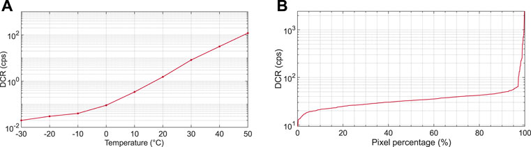
FIGURE 5. Example of variation in DCR for different temperatures for a single SPAD (A), DCR distribution in a SPAD array (B). In this case, hot-pixels are pixels with a DCR higher than 32 cps, corresponding to roughly 3% of the pixels.
The contribution to DCR due to the Poole–Frenkel effect and trap-assisted tunneling does not increase significantly with temperature but instead increases with excess bias. This contribution is usually the dominant one in SPAD architectures with high-doping junctions (i.e., a low VB) [10].
In order to measure DCR, the device is kept in dark and the number of avalanches per second is counted. For SPAD arrays characterization, it is common to report the cumulative distribution function of DCR, as in the example shown in (Figure 5B). This plot depicts the statistics of the DCR among different pixels, in particular the average DCR value and the percentage of noisy SPADs. Noisy pixels, called hot-pixels, are usually defined as the pixels with a DCR higher than twice the median value. Usually, DCR is reported normalized by the active area.
DCR is not correlated with the photon-detection rate, whereas afterpulsing is. During an avalanche, deep level traps present in the detector can capture carriers and release them after a well-defined time (namely the trap release lifetime) [66]. If a carrier is released when the SPAD is fully reverse-biased, a secondary avalanche (afterpulse) is generated. The lifetime can vary from a few nanoseconds to several microseconds and decreases at higher temperatures [67, 68]. Consequently, conversely to DCR, a reduction of temperature has an adverse effect on afterpulsing since it increases the lifetime [10].
The afterpulsing probability is defined as the ratio between the number of afterpulsing events and the total number of events. In order to reduce afterpulsing, after each avalanche, SPADs are kept off for a time window of few nanoseconds (hold-off time, Tho), so that the majority of the trapped carriers are released before rearming the SPAD. However, a long hold-off time lowers the maximum count rate to
The probability of having an afterpulse event depends on the number of carriers that flow during each avalanche. Thus, reducing the avalanche current (i.e., the charge per pulse) is fundamental to decrease the afterpulsing probability. A careful design of the SPAD layout and its frontend circuit can reduce the afterpulsing probability, in fact minimizing the parasitic capacitance associated with the SPAD terminals reduces the avalanche charge. Moreover, the number of deep level traps is lower in high-quality processes, which thus presents a lower afterpulsing probability.
Afterpulsing can be characterized through Time-Correlated Carrier Counting measurements [65, 69]: a histogram of inter-arrival times between two consecutive avalanche pulses is collected. The device must be kept in the dark or under constant illumination so that the event rate is low enough not to limit the maximum inter-arrival time. If no afterpulsing contribution is present, the inter-time trend follows a theoretical exponential distribution (red plot in Figure 6A), which can be subtracted from the measured one (blue plot in Figure 6A). The remaining events are divided by the total counts for computing the afterpulsing probability. The characterization should be repeated at different hold-off times.
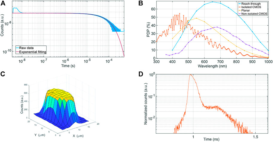
FIGURE 6. Example of inter-arrival time histogram for measuring afterpulsing probability (A), the acquired data are plotted in blue while the exponential decay is plotted in red. PDP of SPADs in different technologies (B). In orange the PDP of a standard isolated CMOS SPAD [71], in yellow the one of a custom planar SPAD [37], in blue the one of a custom reach-trough by Excelitas [72], and in purple the one of a standard non-isolated CMOS SPAD [73]. The ringing present the standard isolated CMOS (orange plot) is due to the oxide layer which causes an interference pattern. Notice that the optimization of the superficial layers, for example by using an antireflection coating, is mandatory to maximize detection efficiency. Results of an active area uniformity test carried out by focusing a laser beam on a spot and scanning the SPAD (C). Example of a SPAD IRF (D).
4.2 Photon Detection Probability
Photon Detection Probability (PDP) is defined as the ratio between the number of detected photons and the number of photons impinging on the active area, thus it characterizes the SPAD light sensitivity. PDP depends on two main parameters: absorption probability and triggering efficiency [70]. The former is the probability that a photon is absorbed within the depleted region and depends on the detector reflectivity, the depth of the junction and the thickness of the depletion region, while the latter is the probability that a photogenerated electron-hole pair triggers a self-sustaining avalanche process and depends on the electric field (it increases with VEX). Although some architectures have an enhanced efficiency in the infrared region to suit specific applications, silicon SPADs have typically high sensitivity in the visible spectrum with a peak in the 300–600 nm range, while their PDP abruptly decreases in the infrared region, as in the examples in Figure 6B. Commonly, PDP is measured by illuminating the device with a light flux at a specific wavelength and the same flux is measured by an instrument with a known responsivity and the two results, after a proper calibration, are compared by normalizing for the areas of the detector. In this way, the result is independent of the geometrical characteristics of the detectors. Note that the light level should be low enough to work in the linear region of the SPAD response, and the DCR should be subtracted from the measured number of events. The measurement is repeated at each wavelength extracting the complete curve (Figure 6B), which offers quantitative information on the SPAD capability of detecting single photons at each wavelength.
4.3 Active Area Uniformity
In order to ascertain SPADs active area uniformity and guard ring functionality, two measurements can be performed: Light Emission Test (LET) and laser beam scanning. During LET, the light emitted during the avalanches is observed with an infrared sensible camera with multi-second acquisition time (e.g., a CCD camera). The light emission is originated from the high field region and shows the uniformity of the field across the active area and possible problems like premature edge breakdown [74].
The extension of the active area can also be measured by focusing a laser beam on a spot smaller than the SPAD under test. The SPAD surface is then scanned recording the count rate per spot position. In this way, it is possible to measure the actual active area diameter and the variation in sensitivity across the device (Figure 6C).
4.4 Timing Jitter
A non-constant time delay between photon absorption and avalanche signal sensing causes a statistical temporal spread of the output pulse. The jitter in the arrival time detected for the single photon is commonly expressed by indicating the Full-Width at Half-Maximum (FWHM) of the SPAD Instrument Response Function (IRF). The IRF can be obtained by illuminating with a pulsed laser the SPAD and building a histogram with the time delays between a reference signal and the SPAD detections. An example of a SPAD IRF is shown in Figure 6D, with its two main components: the Gaussian peak and the exponential tail [75, 76]. Indeed, SPADs show different timing performance depending on the regions in which photons are absorbed. The impact ionization and diffusion of the electron-hole pairs in the depletion region translate into the peak, which is often fit with a Gaussian shape. On the other hand, the drift and diffusion of the minority carriers, generated by photons absorbed in the neutral regions, delay the avalanche triggering causing the exponential tail [76].
The shape of the IRF results distorted if the detected photon rate is too high, because of the pile-up distortion. To prevent this issue, for each laser pulse only one photon should be detected. A non-distorted IRF can be obtained by using a laser power low enough to trigger the SPAD in less than 5% of the pulses, so that, for the Poisson statistics, the probability to have two photons in the same pulse is completely negligible.
Being SPAD jitter strongly influenced by the behavior of the avalanche build-up and spreading phase, by lowering the frontend electronics sensing threshold, allowing to detect pulses when the avalanche is still at the beginning of the build-up phase, the timing jitter reduces, while it increases with detector size. Moreover, the jitter can be reduced by increasing excess biases or by carefully designing the electric field profile [75].
5 Single SPAD Pixels
Typically single SPAD pixel modules provide a digital output pulse every time a photon is detected and can be used for simple counting applications or be optimized targeting low timing jitter, gated or fast-gated operation and high-count rates. Indeed, single SPAD pixels are used in various fields such as single point scanning LiDAR [77], Non-Line of Sight (NLOS) imaging [78, 79], bioimaging and confocal microscopy [80], optical communication and Quantum Key Distribution [81], bucket detector in quantum Ghost Imaging [82], astronomic observation [83], and single-photon source characterization [84].
Single SPAD pixel modules are produced by many companies (e.g., MPD, Excelitas, Hamamatsu, ID Quantique, and PicoQuant) and are available on the market while scientific research is active to improve performance targeting specific applications.
High efficiency, especially in the NIR spectrum, is important when non-visible light must be used. Nevertheless, high PDP in the NIR is typically achieved with deep and thick junctions, which lead to impair the SPAD timing jitter. In [85] 60% PDP at 800 nm is achieved with a reach-trough SPAD by Excelitas that, combined with an integrated frontend circuit, performs only 235 ps timing jitter and an afterpulsing probability below 1.5% at 10 ns deadtime. Even lower jitters of 173 and 83 ps are obtained respectively with a BSI SPAD [86] and SPAD in custom technology connected to an integrated 180 nm CMOS frontend circuit [87] both performing 40% PDP at 800 nm.
Low timing jitter is important in many applications, such as LiDAR and even more in NLOS. The best timing jitter ever reported in literature is presented in [88], with only 7.8 ps jitter FWHM, including SPAD and frontend contributions, but at the expense of a very high DCR (2.8 kcps/µm2) and extremely low PDP (8% peak). Low timing jitter of 27 ps FWHM, along with 60% peak PDP and 0.2 cps/µm2 has been reported in [89].
The capability to fast enabling and disabling the SPAD (i.e., gating operation) is fundamental in NLOS and in many bioimaging techniques. Fast-gated SPAD pixels are reported in [90] (5 ns gate windows and 100 MHz gate frequency), and in [91] with State-of-Art performance in terms of gate window (500 ps) and gate frequency (160 MHz).
High dynamic range and high-count rate are required in LiDAR for background rejection, in quantum communication for achieving high-transmission rates and fluorescence imaging to collect high photon number without pile-up issues. Reducing SPAD deadtime negatively affects the afterpulsing probability, nevertheless low afterpulsing probability below 0.14% and 0.93 ns deadtime are reported in [92], allowing to reach a detection rate exceeding 1 Gcps. A SPAD module designed to surpass the pile-up limit in TCSPC is presented in [93] and its effectiveness is demonstrated in [94]. The module matches the SPAD deadtime with the laser period, providing a uniform probability to detect photons during the entire measurement FSR, thus allowing to obtain TCSPC histograms without distortion, even if the detection rate is higher than 5% (which typically is considered the limit for having negligible distortion).
When SPAD pixels are designed in order to be integrated in SPAD arrays, high fill-factor and small pitch are important parameters to allow the integration of many pixels in a small area. The exploitation of 3D-stacked technologies plays an important role in this route. In [95] the smallest pixel pitch (2.2 µm) ever presented in literature is reported. In the same work, also SPADs with 4 µm pitch are characterized, showing very good results such as 33.5% peak PDP, 2.5 cps median DCR and 88 ps timing jitter.
Expected future trends of SPAD pixels are reported in [96], suggesting that scaling pixel size for larger integrability in imagers will contribute to improving DCR and power consumption, but degrading other figures such as PDP and fill-factor.
6 Conclusion
This review shows the main characteristics, both in terms of technology and figures of merit, of SPADs, photodetectors that are acquiring more and more popularity for SPC and TCSPC applications. It also offers an overview of the advantages and drawbacks of different frontend circuits. This paper is followed by a second part which instead focuses on SPAD arrays, presenting different architectures and their exploitation.
Author Contributions
IC, literature review, writing, review and editing of the full paper. DB, EC, AI, FM, AM., CN, SR, writing of a section of the paper. FV, paper organization, literature review and review of the full paper.
Conflict of Interest
The authors declare that the research was conducted in the absence of any commercial or financial relationships that could be construed as a potential conflict of interest.
Publisher’s Note
All claims expressed in this article are solely those of the authors and do not necessarily represent those of their affiliated organizations, or those of the publisher, the editors and the reviewers. Any product that may be evaluated in this article, or claim that may be made by its manufacturer, is not guaranteed or endorsed by the publisher.
References
2. Zhang L, Chitnis D, Chun H, Rajbhandari S, Faulkner G, O'Brien D, et al. A Comparison of APD- and SPAD-Based Receivers for Visible Light Communications. J Lightwave Technol (2018) 36(12):2435–42. doi:10.1109/jlt.2018.2811180
3. Zappa F, Tisa S, Tosi A, Cova S. Principles and Features of Single-Photon Avalanche Diode Arrays. Sensors Actuators A: Phys (2007) 140:103–12. doi:10.1016/j.sna.2007.06.021
4. Tisa S, Zappa F, Tosi A, Cova S. Electronics for Single Photon Avalanche Diode Arrays. Sensors Actuators A: Phys (2007) 140(1):113–22. doi:10.1016/j.sna.2007.06.022
5. Acerbi F, Gundacker S. Understanding and Simulating SiPMs. In: Nuclear Instruments and Methods in Physics Research Section A: Accelerators, Spectrometers, Detectors and Associated Equipment (Amsterdam, Netherlands: Elsevier), 926 (2019). p. 16–35. doi:10.1016/j.nima.2018.11.118
6. Dauler EA, Grein ME, Kerman AJ, Marsili F, Miki S, Nam SW, et al. Review of Superconducting Nanowire Single-Photon Detector System Design Options and Demonstrated Performance. Opt Eng (2014) 53(8):081907. doi:10.1117/1.oe.53.8.081907
7. Khanduri G. CMOS Image Sensors : Recent Innovations in Imaging Technology. Int J Eng Res Techn (2019) 7(12):3–8. doi:10.17577/IJERTCONV7IS12001
8. Downing M, Hubin N, Kasper M, Jorden P, Pool P, Denney S, et al. A Dedicated L3vision CCD for Adaptive Optics Applications. In: Scientific Detectors for Astronomy. Dordrecht, Netherlands: Springer (2005). p. 321–8.
9. Haitz RH. Model for the Electrical Behavior of a Microplasma. J Appl Phys (1964) 35(5):1370–6. doi:10.1063/1.1713636
10. Haitz RH. Mechanisms Contributing to the Noise Pulse Rate of Avalanche Diodes. J Appl Phys (1965) 36(10):3123–31. doi:10.1063/1.1702936
11. Ghioni M, Cova S, Lacaita A, Ripamonti G. New Silicon Epitaxial Avalanche Diode for Single-Photon Timing at Room Temperature. Electron Lett (1988) 24(24):1476–7. doi:10.1049/el:19881007
12. Cova S, Longoni A, Andreoni A. Towards Picosecond Resolution with Single‐photon Avalanche Diodes. Rev Scientific Instr (1981) 52(3):408–12. doi:10.1063/1.1136594
13. Cova S, Ghioni M, Lacaita A, Samori C, Zappa F. Avalanche Photodiodes and Quenching Circuits for Single-Photon Detection. Appl Opt (1996) 35(12):1956–76. doi:10.1364/AO.35.001956
14. Bondarenko G, Buzhan P, Dolgoshein B, Golovin V, Guschin E, Ilyin A, et al. Limited Geiger-Mode Microcell Silicon Photodiode: New Results. In: Nuclear Instruments and Methods in Physics Research Section A: Accelerators, Spectrometers, Detectors and Associated Equipment. Amsterdam, Netherlands: Elsevier, 442 (2000). p. 187–92. doi:10.1016/s0168-9002(99)01219-x
15. Rochas A, Gani M, Furrer B, Besse PA, Popovic RS, Ribordy G, et al. Single Photon Detector Fabricated in a Complementary Metal-Oxide-Semiconductor High-Voltage Technology. Rev Scientific Instr (2003) 74(7):3263–70. doi:10.1063/1.1584083
16. Rochas A, Gosch M, Serov A, Besse PA, Popovic RS, Lasser T, et al. First Fully Integrated 2-D Array of Single-Photon Detectors in Standard CMOS Technology. IEEE Photon Technol Lett (2003) 15(7):963–5. doi:10.1109/lpt.2003.813387
17. Charbon E, Bruschini C, Lee M-J. 3D-stacked CMOS SPAD Image Sensors: Technology and Applications. In: 2018 25th IEEE International Conference on Electronics, Circuits and Systems (ICECS); 09-12 December 2018; Bordeaux, France (2018).
18. Aull B, Burns J, Chen C, Felton B, Hanson H, Keast C, et al. Laser Radar Imager Based on 3D Integration of Geiger-Mode Avalanche Photodiodes with Two Soi Timing Circuit Layers. In: 2006 IEEE International Solid State Circuits Conference - Digest of Technical Papers; 06-09 February 2006; San Francisco, CA, USA (2006).
19. Pavia JM, Scandini M, Lindner S, Wolf M, Charbon E, Member S. A 1 × 400 Backside-Illuminated SPAD Sensor with 49.7 Ps Resolution, 30 pJ/Sample TDCs Fabricated in 3D CMOS Technology for Near-Infrared Optical Tomography. IEEE J Solid-state Circuits (2015) 50(10):2406–18. doi:10.1109/jssc.2015.2467170
20. Schaefer BE. Search for Gamma ray Burst Counterparts. AIP Conf Proc (1994) 307(1):382. doi:10.1063/1.45900
22. Becker W, Bergmann A, Biscotti G, Koenig K, Riemann I, Kelbauskas L, et al. High-speed FLIM Data Acquisition by Time-Correlated Single-Photon Counting. In: Multiphoton Microscopy in the Biomedical Sciences IV. San Jose, CA: Biomedical Optics 2004 (2004). doi:10.1117/12.529113
23. Bruschini C, Homulle H, Antolovic IM, Burri S, Charbon E. Single-Photon Avalanche Diode Imagers in Biophotonics: Review and Outlook. Light Sci Appl (2019) 8(1):87. doi:10.1038/s41377-019-0191-5
24. Albota MA, Heinrichs RM, Kocher DG, Fouche DG, Player BE, O’Brien ME, et al. Three-dimensional Imaging Laser Radar with a Photon-Counting Avalanche Photodiode Array and Microchip Laser. Appl Opt (2002) 41(36):7671. doi:10.1364/ao.41.007671
25. Bronzi D, Villa F, Tisa S, Tosi A, Zappa F. 100 000 Frames/s 64 × 32 Single-Photon Detector Array for 2-D Imaging and 3-D Ranging. IEEE J Select Top Quan Electron. (2014) 20(6):355–64. doi:10.1109/jstqe.2014.2341562
26. Incoronato A, Severini F, Villa F, Zappa F. Multi-Channel SPAD Chip for Silicon Photonics with Multi-Photon CoIncidence Detection. IEEE J Select Top Quan Electron. (2022) 28(3):1–7. doi:10.1109/jstqe.2021.3134071
27. Tisa S, Villa F, Giudice A, Simmerle G, Zappa F. High-Speed Quantum Random Number Generation Using CMOS Photon Counting Detectors. IEEE J Select Top Quan Electron. (2015) 21(3), 23–29. doi:10.1109/jstqe.2014.2375132
28. Gramuglia F, Muntean A, Venialgo E, Lee M-J, Lindner S, Motoyoshi M, et al. CMOS 3D-Stacked FSI Multi-Channel Digital SIPM for Time-Of-Flight Pet Applications. In: 2020 IEEE Nuclear Science Symposium and Medical Imaging Conference (NSS/MIC); 31 October 2020 - 07 November 2020; Boston, MA, USA (2020).
29. Lecoq P, Gundacker S. SIPM Applications in Positron Emission Tomography: Toward Ultimate Pet Time-Of-Flight Resolution. The Eur Phys J Plus (2021) 136(3). doi:10.1140/epjp/s13360-021-01183-8
30. Bulling AF, Underwood I. X-ray Detection Using Single Photon Avalanche Diodes. In: 2019 IEEE SENSORS; 27-30 October 2019; Montreal, QC, Canada (2019).
31. Antognetti A, Cova S, Longoni A. A Study of the Operation and Performances of an Avalanche Diode as a Single Photon Detector. In: Proceedings 2nd ISPRA Nuclear Electronics Symposium. Luxembourg: Commission of the European Communities (1975). p. 453–6.
32. Cova S, Longoni A, Andreoni A. Avalanche Photodiodes for Single-Photon Detection. In: J Schanda, editor. 9th International Symposiumon Photon Detectors. Budapest: IMEKO-TC2 (1980). p. 82–91.
33. Cova S, Longoni A, Ripamonti G. Physical Phenomena and Performance of Avalanche Photodiodes for Single-Photon Detection, In: 12th European Solid State Device Research Conference; Muenchen, West Germany (1982). p. 15–6.
35. Webb P, McIntyre R. Single Photon Detection with Avalanche Photodiodes. Bull Am Phys Soc (1970) 15:813.
36. Kaneda T, Matsumoto H, Yamaoka T. A Model for Reach‐through Avalanche Photodiodes (RAPD's). J Appl Phys (1976) 47(7):3135–9. doi:10.1063/1.323107
37. Gulinatti A, Rech I, Maccagnani P, Ghioni M, Cova S. Large-area Avalanche Diodes for Picosecond Time-Correlated Photon Counting. In: Proceedings of 35th European Solid-State Device Research Conference ESSDERC 2005; 16-16 September 2005; Grenoble, France (2005).
38. Lacaita A, Ghioni M, Cova S. Double Epitaxy Improves Single-Photon Avalanche Diode Performance. English, Electro Lett (1989) 25(2):841–3. doi:10.1049/el:19890567
39. Ghioni M, Cova S, Lacaita AL, Ripamonti G. Epitaxial Silicon Single Photon Detector with Reduced Carrier Diffusion Effects and Picosecond Resolution. In: 1987 International Electron Devices Meeting; 06-09 December 1987; Washington, DC, USA, 33 (1987). p. 452–5.
40. Gulinatti A, Ceccarelli F, Ghioni M, Rech I. Custom Silicon Technology for SPAD-Arrays with Red-Enhanced Sensitivity and Low Timing Jitter. Opt Express (2021) 29(3):4559. doi:10.1364/oe.413821
41. Gulinatti A, Rech I, Panzeri F, Cammi C, Maccagnani P, Ghioni M, et al. New Silicon Spad Technology for Enhanced Red-Sensitivity, High-Resolution Timing and System Integration. J Mod Opt (2012) 59(17):1489–99. doi:10.1080/09500340.2012.701340
42. Ceccarelli F, Acconcia G, Gulinatti A, Ghioni M, Rech I, Osellame R. Recent Advances and Future Perspectives of Single‐Photon Avalanche Diodes for Quantum Photonics Applications. Adv Quan Tech (2020) 4(2):2000102. doi:10.1002/qute.202000102
43. Ghioni M, Armellini G, Maccagnani P, Rech I, Emsley MK, Unlu MS. Resonant-Cavity-Enhanced Single-Photon Avalanche Diodes on Reflecting Silicon Substrates. IEEE Photon Technol Lett (2008) 20(6):413–5. doi:10.1109/lpt.2008.916926
44. Ghioni M, Gulinatti A, Rech I, Zappa F, Cova S. Progress in Silicon Single-Photon Avalanche Diodes. IEEE J Select Top Quan Electron. (2007) 13(4):852–62. doi:10.1109/jstqe.2007.902088
45. Perenzoni M, Pancheri L, Stoppa D. Compact SPAD-Based Pixel Architectures for Time-Resolved Image Sensors. Sensors (2016) 16(5):745. doi:10.3390/s16050745
46. Niclass C, Matsubara H, Soga M, Ohta M, Ogawa M, Yamashita T. A NIRsensitivity-Enhanced Single-Photon Avalanche Diode in 0.18 1mCMOS. In: Proceedings of the International Image Sensor Workshop; 8-11 June, 2015; Vaals, The Netherlands (2015).
47. Zappa F, Tosi A, Mora AD, Tisa S. Spice Modeling of Single Photon Avalanche Diodes. Sensors Actuators A: Phys (2009) 153(2):197–204. doi:10.1016/j.sna.2009.05.007
48. Panglosse A, Martin-Gonthier P, Marcelot O, Virmontois C, Saint-Pe O, Magnan P. Dark Count Rate Modeling in Single-Photon Avalanche Diodes for Space Lidar Applications. In: 2019 17th IEEE International New Circuits and Systems Conference (NEWCAS); 23-26 June 2019; Munich, Germany (2019).
49. Sun F, Xu Y, Wu Z, Zhang J. A Simple Analytic Modeling Method for SPAD Timing Jitter Prediction. IEEE J Electron Devices Soc (2019) 7:261–7. doi:10.1109/jeds.2019.2895151
50. Zhao T, Sun F, Xu Y, Li B, Li D. An Improved Behavioral Simulation Model for Afterpulsing Phenomenon. In: 2018 China Semiconductor Technology International Conference (CSTIC); 11-12 March 2018; Shanghai, China (2018).
51. Giustolisi G, Mita R, Palumbo G. Verilog-A Modeling of SPAD Statistical Phenomena. In: 2011 IEEE International Symposium of Circuits and Systems (ISCAS); 15-18 May 2011; Rio de Janeiro, Brazil (2011). doi:10.1109/iscas.2011.5937680
52. Savuskan V, Javitt M, Visokolov G, Brouk I, Nemirovsky Y. Selecting Single Photon Avalanche Diode (SPAD) Passive-Quenching Resistance: An Approach. IEEE Sensors J (2013) 13(6):2322–8. doi:10.1109/jsen.2013.2253603
53. Hayat MM, Itzler MA, Ramirez DA, Rees GJ. Model for Passive Quenching of SPADs. In: SPIE Proceedings. San Francisco, CA: SPIE OPTO (2010).
54. Jungwirth M, Dervic A, Zimmermann H. Integrated High Voltage Active Quenching Circuit in 150nm CMOS Technology. In: 2020 Austrochip Workshop on Microelectronics (Austrochip); 07-07 October 2020; Vienna, Austria (2020).
55. Cova S, Longoni A, Ripamonti G. Active-Quenching and Gating Circuits for Single-Photon Avalanche Diodes (SPADs). IEEE Trans Nucl Sci (1982) 29:599–601. doi:10.1109/tns.1982.4335917
56. Ceccarelli F, Acconcia G, Gulinatti A, Ghioni M, Rech I. Fully Integrated Active Quenching Circuit Driving Custom-Technology SPADs with 6.2-NS Dead Time. IEEE Photon Technol Lett (2019) 31(1):102–5. doi:10.1109/lpt.2018.2884740
57. Tisa S, Guerrieri F, Zappa F. Variable-Load Quenching Circuit for Single-Photon Avalanche Diodes. Opt Express (2008) 16:2232–44. doi:10.1364/oe.16.002232
58. Portaluppi D, Conca E, Villa F. 32 × 32 CMOS SPAD Imager for Gated Imaging, Photon Timing, and Photon Coincidence. IEEE J Select Top Quan Electron. (2018) 24(2):1–6. doi:10.1109/jstqe.2017.2754587
59. Vornicu I, Carmona-Galán R, Pérez-Verdú B, Rodríguez-Vázquez Á. Compact CMOS Active Quenching/recharge Circuit for SPAD Arrays. Int J Circ Theor Appl (2015) 44(4):917–28. doi:10.1002/cta.2113
60. Henderson RK, Johnston N, Hutchings SW, Gyongy I, Abbas TA, Dutton N, et al. 5.7 A 256×256 40nm/90nm CMOS 3D-Stacked 120db Dynamic-Range Reconfigurable Time-Resolved Spad Imager. In: 2019 IEEE International Solid- State Circuits Conference - (ISSCC); 17-21 February 2019; San Francisco, CA, USA (2019).
61. Mahmoudi H, Hofbauer M, Goll B, Zimmermann H. Noise and Breakdown Characterization of SPAD Detectors with Time-Gated Photon-Counting Operation. Sensors (2021) 21(16):5287. doi:10.3390/s21165287
62. Burri S, Maruyama Y, Michalet X, Regazzoni F, Bruschini C, Charbon E. Architecture and Applications of a High Resolution Gated SPAD Image Sensor. Opt Express (2014) 22(14):17573. doi:10.1364/oe.22.017573
63. Gallivanoni A, Rech I, Ghioni andM. Progress in Quenching Circuits for Single Photon Avalanche Diodes. IEEE Trans Nucl Sci (2010) 57(6):3815–26. doi:10.1109/tns.2010.2074213
64. Richardson JA, Grant LA, Henderson RK. Low Dark Count Single-Photon Avalanche Diode Structure Compatible with Standard Nanometer Scale CMOS Technology. IEEE Photon Technol Lett (2009) 21(14):1020–2. doi:10.1109/lpt.2009.2022059
65. Lim KT, Kim H, Kim J, Cho G. Effect of Electric Field on Primary Dark Pulses in Spads for Advanced Radiation Detection Applications. Nucl Eng Techn (2021) 53(2):618–25. doi:10.1016/j.net.2020.07.006
66. Cova S, Lacaita A, Ripamonti G. Trapping Phenomena in Avalanche Photodiodes on Nanosecond Scale. IEEE Electron Device Lett (1991) 12(12):685–7. doi:10.1109/55.116955
67. Giustolisi G, Mita R, Palumbo G. Behavioral Modeling of Statistical Phenomena of Single-Photon Avalanche Diodes. Int J Circ Theor Appl (2011) 40(7):661–79. doi:10.1002/cta.748
68. Stipcevic M, Wang D, Ursin R. Characterization of a Commercially Available Large Area, High Detection Efficiency Single-Photon Avalanche Diode. J Lightwave Technol (2013) 31(23):3591–6. doi:10.1109/jlt.2013.2286422
69. Giudice A, Ghioni M, Cova S, Zappa F. A Process and Deep Level Evaluation Tool: Afterpulsing in Avalanche Junctions. In: ESSDERC '03. 33rd Conference on European Solid-State Device Research, 2003; 16-18 September 2003; Estoril, Portugal (2003). p. 347–50.
71. Villa F, Bronzi D, Zou Y, Scarcella C, Boso G, Tisa S, et al. CMOS SPADS with up to 500 μm Diameter and 615 55% Detection Efficiency at 420 Nm. J Mod Opt (2014) 61(2):102–15. 616.
72. Dautet H, Deschamps P, Dion B, MacGregor AD, MacSween D, McIntyre RJ, et al. Photon Counting Techniques with Silicon Avalanche Photodiodes. Appl Opt (1993) 32(21):3894–900. doi:10.1364/ao.32.003894
73. Karami MA, Gersbach M, Yoon H-J, Charbon E. A New Single-Photon Avalanche Diode in 90nm Standard CMOS Technology. Opt Express (2010) 18(21):22158–622 22166, Oct. doi:10.1364/oe.18.022158
74. Knezevic T, Karavidas A, Nanver LK, Krakers M, Agarwal V, Hueting R, et al. Investigation of Light-Emission and Avalanche-Current Mechanisms in Pureb SPAD Devices. In: Fifth Conference on Sensors, MEMS, and Electro-Optic Systems; 8 Oct 2018 to 10 Oct 2018; Skukuza, South Africa (2019).
75. Lacaita A, Cova S, Ghioni M, Zappa F. Single-photon Avalanche Diode with Ultrafast Pulse Response Free from Slow Tails. IEEE Electron Device Lett (1993) 14:360–2. doi:10.1109/55.225573
76. Ripamonti G, Cova S. Carrier Diffusion Effects in the Time-Response of a Fast Photodiode. Solid-State Electro (1985) 28(9):925–31.
77. Turpin A, Musarra G, Tonolini F, Murray-Smith R, Faccio D. Single Photon and Single Pixel Technology for Computational Lidar. In: Laser Congress 2019 (ASSL, LAC, LS&C). Vienna, Austria (2019).
78. Buttafava M, Zeman J, Tosi A, Eliceiri K, Velten A. Non-line-of-sight Imaging Using a Time-Gated Single Photon Avalanche Diode. Opt Express (2015) 23(16):20997–1011. doi:10.1364/OE.23.020997
79. Musarra G, Lyons A, Conca E, Altmann Y, Villa F, Zappa F, et al. Non-Line-of-sight Three-Dimensional Imaging with a Single-Pixel Camera. Phys Rev Appl (2019) 12(1). doi:10.1103/physrevapplied.12.011002
80. Li LQ, Davis LM. Single Photon Avalanche Diode for Single Molecule Detection. Rev Scientific Instr (1993) 64(6):1524–9. doi:10.1063/1.1144463
81. Gordon KJ, Fernandez V, Townsend PD, Buller GS. A Short Wavelength GigaHertz Clocked Fiber-Optic Quantum Key Distribution System. IEEE J Quan Electron. (2004) 40(7):900–8. doi:10.1109/JQE.2004.830182
82. Moreau P-A, Toninelli E, Gregory T, Padgett MJ. Ghost Imaging Using Optical Correlations. Laser Photon Rev (2017) 12(1):1700143. doi:10.1002/lpor.201700143
83. Barbieri C, Naletto G, Occhipinti T, Facchinetti C, Verroi E, Giro E, et al. AquEYE, a Single Photon Counting Photometer for Astronomy. J Mod Opt (2009) 56(2-3):261–72. doi:10.1080/09500340802450565
84. Brida G, Degiovanni IP, Genovese M, Piacentini F, Traina P, Della Frera A, et al. An Extremely Low-Noise Heralded Single-Photon Source: A Breakthrough for Quantum Technologies. Appl Phys Lett (2012) 101(22):221112. doi:10.1063/1.4768288
85. Farina S, Labanca I, Acconcia G, Ghioni M, Rech I. 10-nanosecond Dead Time and Low Afterpulsing with a Free-Running Reach-Through Single-Photon Avalanche Diode. Rev Scientific Instr (2022) 93(5):053102. doi:10.1063/5.0086312
86. Ito K, Otake Y, Kitano Y, Matsumoto A, Yamamoto J, Ogasahara T, et al. A Back Illuminated 10μm SPAD Pixel Array Comprising Full Trench Isolation and Cu-Cu Bonding with over 14% PDE at 940nm. In: 2020 IEEE International Electron Devices Meeting (IEDM); 12-18 December 2020; San Francisco, CA, USA (2020).
87. Ceccarelli F, Acconcia G, Gulinatti A, Ghioni M, Rech I. 83-PS Timing Jitter with a Red-Enhanced SPAD and a Fully Integrated Front End Circuit. IEEE Photon Technol Lett (2018) 30(19):1727–30. doi:10.1109/lpt.2018.2867805
88. Nolet F, Parent S, Roy N, Mercier M-O, Charlebois S, Fontaine R, et al. Quenching Circuit and SPAD Integrated in CMOS 65 Nm with 7.8 PS FWHM Single Photon Timing Resolution. Instruments (2018) 2(4):19. doi:10.3390/instruments2040019
89. Sanzaro M, Gattari P, Villa F, Tosi A, Croce G, Zappa F. Single-Photon Avalanche Diodes in a 0.16 μm BCD Technology with Sharp Timing Response and Red-Enhanced Sensitivity. IEEE J Select Top Quan Electron. (2018) 24(2):1–9. doi:10.1109/jstqe.2017.2762464
90. Jiang W, Chalich Y, Scott R, Deen MJ. Time-gated and Multi-junction SPADs in Standard 65 Nm CMOS Technology. IEEE Sensors J (2021) 21(10):12092–103. doi:10.1109/jsen.2021.3063319
91. Renna M, Ruggeri A, Sanzaro M, Villa F, Zappa F, Tosi A. High Detection Rate Fast-Gated CMOS Single-Photon Avalanche Diode Module. IEEE Photon J. (2020) 12(5):1–12. doi:10.1109/jphot.2020.3017092
92. Severini F, Cusini I, Berretta D, Pasquinelli K, Incoronato A, Villa F. SPAD Pixel with Sub-NS Dead-Time for High-Count Rate Applications. IEEE J Select Top Quan Electron. (2022) 28(2):1–8. doi:10.1109/jstqe.2021.3124825
93. Farina S, Acconcia G, Labanca I, Ghioni M, Rech I. Toward Ultra-fast Time-Correlated Single-Photon Counting: A Compact Module to Surpass the Pile-Up Limit. Rev Scientific Instr (2021) 92(6):063702. doi:10.1063/5.0044774
94. Farina S, Labanca I, Acconcia G, Ghezzi A, Farina A, D’Andrea C, et al. Above Pile-Up Fluorescence Microscopy with a 32 MC/s Single-Channel Time-Resolved SPAD System. Opt Lett (2021) 47(1):82. doi:10.1364/ol.444815
95. Morimoto K, Charbon E. High Fill-Factor Miniaturized SPAD Arrays with a Guard-Ring-Sharing Technique. Opt Express (2020) 28:13068–80. doi:10.1364/oe.389216
Keywords: single-photon avalanche diode (SPAD), quenching circuits, SPAD arrays, single photon counting (SPC), time-correlated single-photon counting (TCSPC)
Citation: Cusini I, Berretta D, Conca E, Incoronato A, Madonini F, Maurina AA, Nonne C, Riccardo S and Villa F (2022) Historical Perspectives, State of art and Research Trends of Single Photon Avalanche Diodes and Their Applications (Part 1: Single Pixels). Front. Phys. 10:906675. doi: 10.3389/fphy.2022.906675
Received: 28 March 2022; Accepted: 10 June 2022;
Published: 30 June 2022.
Edited by:
Jelena Ninkovic, Halbleiterlabor of the Max-Planck-Society, GermanyReviewed by:
Adriano Lai, National Institute of Nuclear Physics of Cagliari, ItalyGabriele D'Amen, Brookhaven National Laboratory (DOE), United States
Copyright © 2022 Cusini, Berretta, Conca, Incoronato, Madonini, Maurina, Nonne, Riccardo and Villa. This is an open-access article distributed under the terms of the Creative Commons Attribution License (CC BY). The use, distribution or reproduction in other forums is permitted, provided the original author(s) and the copyright owner(s) are credited and that the original publication in this journal is cited, in accordance with accepted academic practice. No use, distribution or reproduction is permitted which does not comply with these terms.
*Correspondence: Iris Cusini, iris.cusini@polimi.it