Computer Organization 5th Module
5.1 SOME FUNDAMENTAL CONCEPTS
To execute an instruction, processor has to perform following 3 steps:
Fetch contents of memory-location pointed to by PC. Content of this location is an instruction
to be executed. The instructions are loaded into IR, Symbolically, this operation is written as: IR[[PC]]
Increment PC by 4.
Carry out the actions specified by instruction (in the IR).
The first 2 steps are referred to as Fetch Phase.
The operation specified by an instruction can be carried out by performing one or more of the following actions:
Read the contents of a given memory-location and load them into a register.
Read data from one or more registers.
Perform an arithmetic or logic operation and place the result into a register.
Store data from a register into a given memory-location.
The hardware-components needed to perform these actions are shown in Figure 5.1.
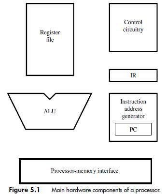
by the instruction (loaded in the IR).
Register R0 through R(n-1) are the Processor Registers.
5.2 SINGLE BUS ORGANIZATION
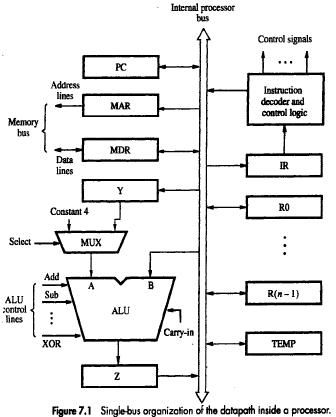
ALU and all the registers are interconnected via a Single Common Bus (Figure 7.1).
Data & address lines of the external memory-bus is connected to the internal processor-bus via MDR & MAR respectively. (MDR Memory Data Register, MAR Memory Address Register).
MDR has 2 inputs and 2 outputs. Data may be loaded
into MDR either from memory-bus (external) or
from processor-bus (internal).
MAR‟s input is connected to internal-bus;
Instruction Decoder & Control Unit is responsible for
issuing the control-signals to all the units inside the processor.
implementing the actions specified
Only processor can access 3 registers Y, Z& Temp for temporary storage during program-execution.
In ALU, 1) „A‟ input gets the operand from the output of the multiplexer (MUX).
„B‟ input gets the operand directly from the processor-bus.
There are 2 options provided for „A‟ input of the ALU.
MUX is used to select one of the 2 inputs.
MUX selects either
output of Y or
constant-value 4( which is used to increment PC content).
An instruction is executed by performing one or more of the following operations:
Transfer a word of data from one register to another or to the ALU.
Perform arithmetic or a logic operation and store the result in a register.
Fetch the contents of a given memory-location and load them into a register.
Store a word of data from a register into a given memory-location.
Disadvantage: Only one data-word can be transferred over the bus in a clock cycle.
Solution: Provide multiple internal-paths. Multiple paths allow several data-transfers to take place in parallel
5.3 REGISTER TRANSFERS
Instruction execution involves a sequence of steps in which data are transferred from one register to
another.
For each register, two control-signals are used: Riin & Riout. These are called Gating Signals.
Riin=1 data on bus is loaded into Ri.
For example, MOVE R1, R2; This transfers the contents of register R1 to register R2. This can be accomplished as follows:
Enable the output of registers R1 by setting R1out to 1 (Figure 7.2). This places the contents of R1 on processor-bus.
Enable the input of register R2 by setting R2outto 1.
All operations and data transfers within the processor take place within time-periods defined by the processor-clock.
The control-signals that govern a particular transfer are asserted at the start of the clock cycle.
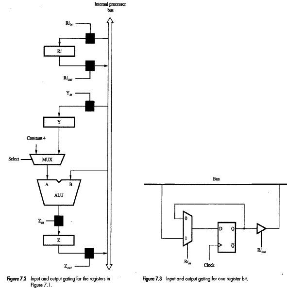
5.3.1 Input & Output Gating for one Register Bit
A 2-input multiplexer is used to select the data applied to the input of an edge-triggered D flip-flop.
Riin=1 mux selects data on bus. This data will be loaded into flip-flop at rising-edge of clock.
Q output of flip-flop is connected to bus via a tri-state gate. Riout=0 gate's output is in the high-impedance state.
Riout=1 the gate drives the bus to 0 or 1, depending on the value of Q.
5.3.2 PERFORMING AN ARITHMETIC OR LOGIC OPERATION
The ALU performs arithmetic operations on the 2 operands applied to its A and B inputs.
One of the operands is output of MUX;
The result (produced by the ALU) is stored temporarily in register Z.
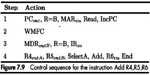
The sequence of operations for [R3][R1]+[R2] is as follows:
R1out, Yin
R2out, SelectY, Add, Zin
Zout, R3in
Instruction execution proceeds as follows:
Step 1 --> Contents from register R1 are loaded into register Y.
Step2 --> Contents from Y and from register R2 are applied to the A and B inputs of ALU; Addition is performed &
Result is stored in the Z register.
Step 3 --> The contents of Z register is stored in the R3 register.
The signals are activated for the duration of the clock cycle corresponding to that step. All other signals are inactive.
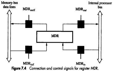
5.3.3 CONTROL-SIGNALS OF MDR
The MDR register has 4 control-signals (Figure 7.4):
MDRin & MDRoutcontrol the connection to the internal processor data bus &
MDRinE & MDRoutEcontrol the connection to the memory Data bus.
MAR register has 2 control-signals.
MARin controls the connection to the internal processor address bus &
MARout controls the connection to the memory address bus.
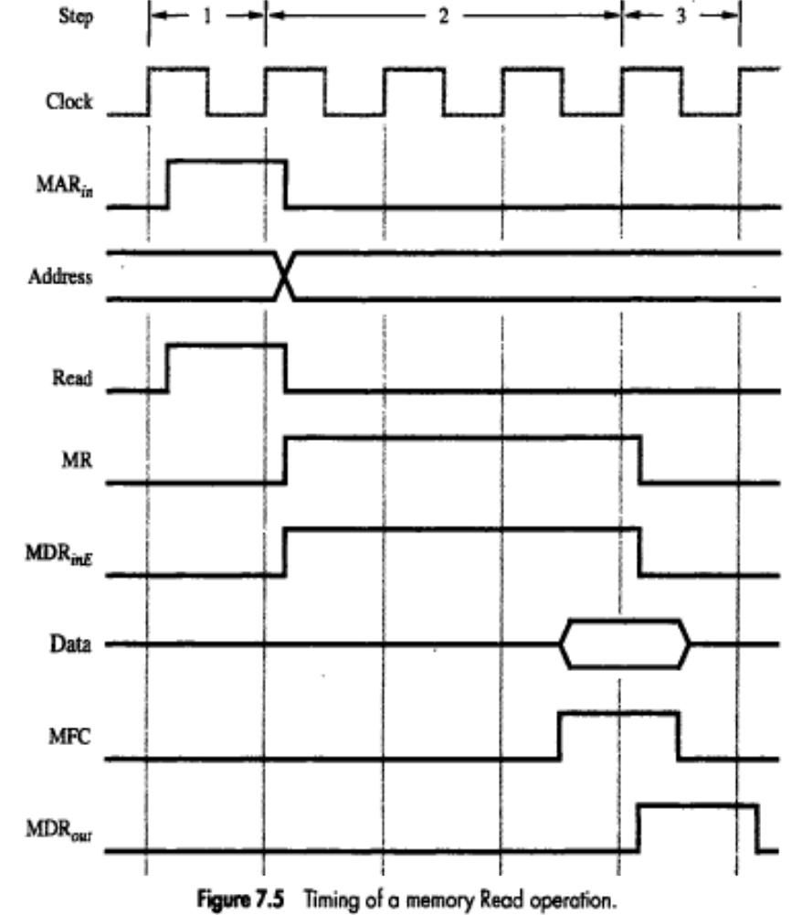
5.4 FETCHING A WORD FROM MEMORY
To fetch instruction/data from memory, processor transfers required address to MAR. At the same time, processor issues Read signal on control-lines of memory-bus.
When requested-data are received from memory, they are stored in MDR. From MDR, they are
transferred to other registers.
The response time of each memory access varies (based on cache miss, memory-mapped I/O). To accommodate this, MFC is used. (MFC Memory Function Completed).
MFC is a signal sent from addressed-device to the processor. MFC informs the processor that the requested operation has been completed by addressed-device.
Consider the instruction Move (R1),R2. The sequence of steps is (Figure 7.5):
R1out, MARin, Read ;desired address is loaded into MAR & Read command is issued.
|
2) |
MDRinE, WMFC |
;load MDR from memory-bus & Wait for MFC response from memory. |
|
3) |
MDRout, R2in |
;load R2 from MDR. |
where WMFC=control-signal that causes processor's control.
circuitry to wait for arrival of MFC signal.
Storing a Word in Memory
Consider the instruction MOVE R2,(R1). This requires the following sequence:
|
1) |
R1out, MARin |
;desired
address is loaded into MAR. |
|
2) |
R2out, MDRin, Write |
;data to be written are loaded into MDR & Write command is
issued. |
|
3) |
MDRoutE, WMFC |
;load data into memory-location pointed by R1 from MDR. |
5.5 EXECUTION OF A COMPLETE INSTRUCTION
Consider the instruction ADD (R3),R1 which adds the contents of a memory-location pointed by R3 to register R1. Executing this instruction requires the following actions:
Fetch the instruction.
Fetch the first operand.
Perform the addition &
Load the result into R1.
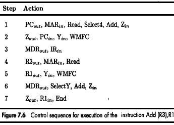
Instruction execution proceeds as follows:
loading contents of PC into MAR & sending a Read request to memory.
The Select signal is set to Select4, which causes the Mux to select constant 4. This value is added to operand at input B (PC‟s content), and the result is stored in Z.
Step2--> Updated value in Z is moved to PC. This completes the PC increment operation and PC will now point to next instruction.
Step3--> Fetched instruction is moved into MDR and then to IR.
The step 1 through 3 constitutes the Fetch Phase.
At the beginning of step 4, the instruction decoder interprets the contents of the IR. This enables the control circuitry to activate the control-signals for steps 4 through 7. The step 4 through 7 constitutes the Execution Phase.
Step4--> Contents of R3 are loaded into MAR & a memory read signal is issued.
Step5--> Contents of R1 are transferred to Y to prepare for addition.
Step6--> When Read operation is completed, memory-operand is available in MDR, and the addition is performed.
Step7--> Sum is stored in Z, then transferred to R1.The End signal causes a new instruction fetch cycle to begin by returning to step1.
5.5.1 BRANCHING INSTRUCTIONS
Control sequence for an unconditional branch instruction is as follows:
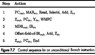
Instruction execution proceeds as follows:
Step 1-3--> The processing starts & the fetch phase ends in step3.
Step 4--> The offset-value is extracted from IR by instruction-decoding circuit.
Since the updated value of PC is already available in register , the offset X is gated onto the bus, and an addition operation is performed.
Step 5--> the result, which is the branch-address, is loaded into the PC.
The branch instruction loads the branch target address in PC so that PC will fetch the next instruction from the branch target address.
The branch target address is usually obtained by adding the offset in the contents of PC.
The offset X is usually the difference between the branch target-address and the address immediately following the branch instruction.
In case of conditional branch,
we have to check the status of the condition-codes before loading a new value into the PC.
e.g.: Offset-field-of-IRout, Add, Zin, If N=0 then nd
If N=0, processor returns to step 1 immediately after step 4.
If N=1, step 5 is performed to load a new value into PC
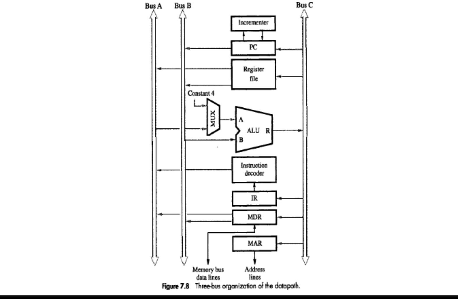
5.6 MULTIPLE BUS ORGANIZATION
Disadvantage of Single-bus organization: Only one data-word can be transferred over the bus in a clock cycle. This increases the steps required to complete the execution of the instruction Solution: To reduce the number of steps, most processors provide multiple internal-paths. Multiple
paths enable several transfers to take place in parallel.
As shown in fig 7.8, three buses can be used to connect registers and the ALU of the processor.
All general-purpose registers are grouped into a single block called the Register File.
Register-file has 3 ports:
Two output-ports allow the contents of 2 different registers to be simultaneously placed on buses A & B.
Third input-port allows data on bus C to be loaded into a third register during the same clock-cycle.
Buses A and B are used to transfer source-operands to A & B inputs of ALU.
The result is transferred to destination over bus C.
Incrementer Unit is used to increment PC by 4.
Instruction execution proceeds as follows: Step 1--> Contents of PC are
passed through ALU using R=B control-signal &
loaded into MAR to start memory Read operation. At the same time, PC is incremented by 4. Step2--> Processor waits for MFC signal from memory.
Step3--> Processor loads requested-data into MDR, and then transfers them to IR. Step4--> The instruction is decoded and add operation takes place in a single step.
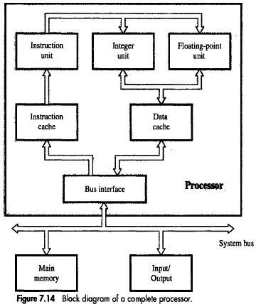
5.7 COMPLETE PROCESSOR
This has separate processing-units to deal with integer data and floating-point data. Integer Unit To process integer data. (Figure 7.14).
Floating Unit To process floating –point data.
Data-Cache is inserted between these processing-units & main-memory.
Instruction-Unit fetches instructions
from an instruction-cache or
from main-memory when desired instructions are not already in cache.
Processor is connected to system-bus &
hence to the rest of the computer by means of a Bus Interface.
Using separate caches for instructions & data is common practice in many processors today.
A processor may include several units of each type to increase the potential for concurrent operations.
The 80486 processor has 8-kbytes single cache for both instruction and data.
Whereas the Pentium processor has two separate 8 kbytes caches for instruction and data.
Note:
To execute instructions, the processor must have some means of generating the control-signals. There are two approaches for this purpose:
1) Hardwired control and 2) Microprogrammed control.
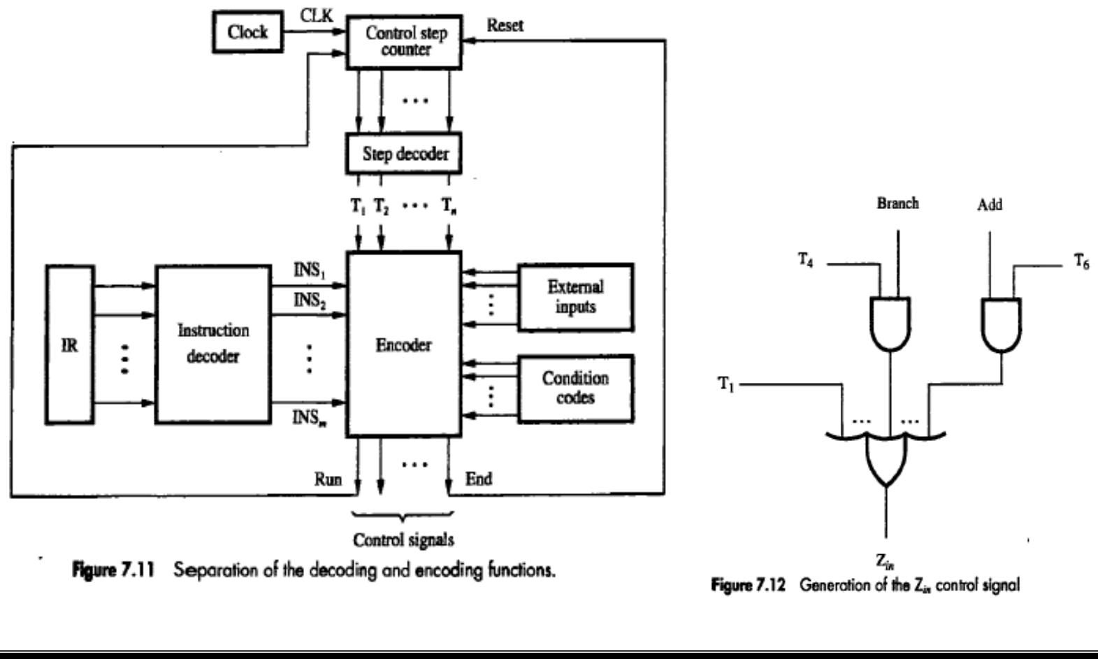
5.8 HARDWIRED CONTROL
Hardwired control is a method of control unit design (Figure 7.11).
The control-signals are generated by using logic circuits such as gates, flip-flops, decoders etc.
Decoder/Encoder Block is a combinational-circuit that generates required control-outputs depending on state of all its inputs.
Instruction Decoder
It decodes the instruction loaded in the IR.
If IR is an 8 bit register, then instruction decoder generates 28(256 lines); one for each instruction.
It consists of a separate output-lines INS1through INSm for each machine instruction.
According to code in the IR, one of the output-lines INS1 through INSm is set to 1, and all other lines are set to 0.
Step-Decoder provides a separate signal line for each step in the control sequence.
Encoder
It gets the input from instruction decoder, step decoder, external inputs and condition codes.
It uses all these inputs to generate individual control-signals: Yin, PCout, Add, End and so on.
For example (Figure 7.12), ZIN=T1+T6.ADD+T4.BR
This signal is asserted during time-slot T1 for all instructions. During T6 for an Add instruction. During T4 for unconditional branch instruction
When RUN=1, counter is incremented by 1 at the end of every clock cycle.
After execution of each instruction, end signal is generated. End signal resets step counter.
Sequence of operations carried out by this machine is determined by wiring of logic circuits, hence the name “hardwired”.
Advantage: Can operate at high speed.
Disadvantages:
Since no. of instructions/control-lines is often in hundreds, the complexity of control unit is very high.
It is costly and difficult to design.
The control unit is inflexible because it is difficult to change the design.
5.8.1 HARDWIRED CONTROL VS MICROPROGRAMMED CONTROL
|
Attribute |
|
|
Hardwired
Control |
Microprogrammed
Control |
|
|||||||
|
Definition |
|
|
Hardwired control is a control |
Micro programmed control is a control |
||||||||
|
|
|
|
mechanism
to generate control- |
mechanism
to generate control-signals |
||||||||
|
|
|
|
signals by
using gates, flip- |
by
using a memory called control store |
||||||||
|
|
|
|
flops, |
decoders, |
and other |
(CS), which
contains the control- |
||||||
|
|
|
|
digital circuits. |
|
|
signals. |
|
|
|
|
||
|
Speed |
|
|
Fast |
|
|
|
Slow |
|
|
|
|
|
|
Control
functions |
Implemented in hardware. |
Implemented in software. |
|
|
||||||||
|
Flexibility |
|
|
Not |
flexible |
to |
accommodate |
More flexible, to accommodate new |
|||||
|
|
|
|
new |
system |
specifications or |
system
specification or new instructions |
||||||
|
|
|
|
new
instructions. |
|
redesign
is required. |
|
|
|||||
|
Ability
to |
handle large |
Difficult. |
|
|
Easier. |
|
|
|
|
|||
|
or complex |
instruction |
|
|
|
|
|
|
|
|
|
|
|
|
sets |
|
|
|
|
|
|
|
|
|
|
|
|
|
Ability |
to |
support |
Very difficult. |
|
|
Easy. |
|
|
|
|
|
|
|
operating |
systems & |
|
|
|
|
|
|
|
|
|
|
|
|
diagnostic features |
|
|
|
|
|
|
|
|
|
|
||
|
Design
process |
Complicated. |
|
|
Orderly and systematic. |
|
|
||||||
|
Applications |
|
Mostly RISC microprocessors. |
Mainframes, some microprocessors. |
|
||||||||
|
Instructionset
size |
Usually under 100 instructions. |
Usually over 100 instructions. |
|
|||||||||
|
ROM size |
|
|
- |
|
|
|
2K |
to |
10K |
by |
20-400 |
bit |
|
|
|
|
|
|
|
|
microinstructions. |
|
|
|
||
|
Chip area
efficiency |
Uses least area. |
|
Uses more area. |
|
|
|
||||||
|
|
|
|
|
|
|
|
||||||
5.9 MICROPROGRAMMED CONTROL
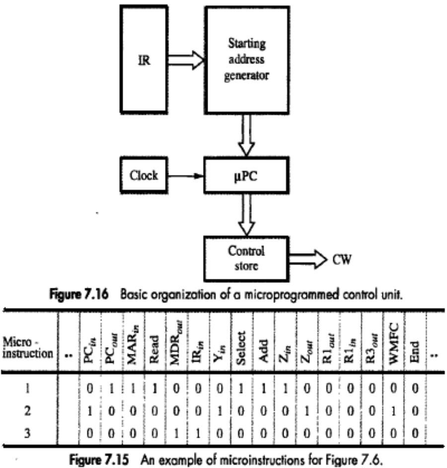
Microprogramming is a method of control unit design (Figure 7.16).
Control-signals are generated by a program similar to machine language programs.
Control Word(CW) is a word whose individual bits represent various control-signals (like Add, PCin).
Each of the control-steps in control sequence of an instruction defines a unique combination of 1s & 0s in CW.
Individual control-words in microroutine are referred to as microinstructions(Figure 7.15).
A sequence of CWs corresponding to control-sequence of a machine instruction constitutes the microroutine.
The microroutines for all instructions in the instruction-set of a computer are stored in a special memory called the Control Store (CS).
Control-unit generates control-signals for any instruction by sequentially reading CWs of corresponding microroutine from CS.
µPC is used to read CWs sequentially from CS. (µPC Microprogram Counter).
Every time new instruction is loaded into IR, o/p of Starting Address Generator is loaded into µPC.
Then, µPC is automatically incremented by clock; causing successive microinstructions to be read from CS.Hence, control-signals are delivered to various parts of processor in correct sequence.
Advantages
It simplifies the design of control unit. Thus it is both, cheaper and less error prone implement.
Control functions are implemented in software rather than hardware.
The design process is orderly and systematic.
More flexible, can be changed to accommodate new system specifications or to correct the design
errors quickly and cheaply.
Complex function such as floating point arithmetic can be realized efficiently.
Disadvantages
• A microprogrammed control unit is somewhat slower than the hardwired control unit, because time is
required to access the microinstructions from CM.
The flexibility is achieved at some extra hardware cost due to the control memory and its access circuitry.
5.9.1 ORGANIZATION OF MICROPROGRAMMED CONTROL UNIT TO SUPPORT CONDITIONAL BRANCHING
Drawback of previous Microprogram control:
It cannot handle the situation when the control unit is required to check the status of the
condition codes or external inputs to choose between alternative courses of action.
Solution:
Use conditional branch microinstruction.
In case of conditional branching, microinstructions specify which of the external inputs, condition-codes should be checked as a condition for branching to take place.
Starting and Branch Address Generator Block loads a new address into µPC when a microinstruction instructs it to do so (Figure 7.18).
To allow implementation of a conditional branch, inputs to this block consist of
external inputs and condition-codes &
contents of IR.
µPC is incremented every time a new microinstruction is fetched from microprogram memory except in following situations:
1) When a new instruction is loaded into IR, µPC is loaded with starting-address of microroutine for that instruction.
2) When a Branch microinstruction is encountered and branch condition is satisfied, µPC is loaded with branch-address.
3) When an End microinstruction is encountered, µPC is loaded with address of first CW in microroutine for instruction fetch cycle.
5.10 MICROINSTRUCTIONS
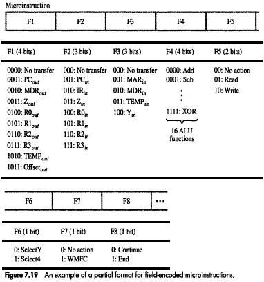
A simple way to structure microinstructions is to assign one bit position to each control-signal required in the CPU.
There are 42 signals and hence each microinstruction will have 42 bits.
Drawbacks of microprogrammed control:
Assigning individual bits to each control-signal results in long microinstructions because
the number of required signals is usually large.
2) Available bit-space is poorly used because
only a few bits are set to 1 in any given microinstruction.
Solution: Signals can be grouped because
Most signals are not needed simultaneously.
Many signals are mutually exclusive. E.g. only 1 function of ALU can be activated at a time. For ex: Gating signals: IN and OUT signals (Figure 7.19).
Control-signals: Read, Write.
ALU signals: Add, Sub, Mul, Div, Mod.
Grouping control-signals into fields requires a little more hardware because
decoding-circuits must be used to decode bit patterns of each field into individual control-signals.
Advantage: This method results in a smaller control-store (only 20 bits are needed to store the patterns for the 42 signals).

TECHNIQUES OF GROUPING OF CONTROL-SIGNALS
The grouping of control-signal can be done either by using
Vertical organization &
Horizontal organisation.
|
|
Vertical Organization |
|
Horizontal Organization |
|
|
||||
|
Highly encoded schemes that use compact |
The minimally encoded scheme in which many |
|
|||||||
|
codes
to specify only a small number of control |
resources
can be controlled with a single |
|
|||||||
|
functions
in each microinstruction are referred |
microinstruction is |
called |
a |
horizontal |
|||||
|
to
as a vertical organization. |
|
|
organization. |
|
|
|
|||
|
Slower operating-speeds. |
|
|
Useful when higher operating-speed is desired. |
|
|||||
|
Short formats. |
|
|
|
Long formats. |
|
|
|
||
|
Limited |
ability |
to |
express |
parallel |
Ability to express a high degree of parallelism. |
|
|||
|
microoperations. |
|
|
|
|
|
|
|
||
|
Considerable encoding of
the control |
Little encoding of the control information. |
|
|||||||
|
information. |
|
|
|
|
|
|
|
||
5.10.1MICROPROGRAM SEQUENCING
The task of microprogram sequencing is done by microprogram sequencer.
Two important factors must be considered while designing the microprogram sequencer:
The size of the microinstruction &
The address generation time.
The size of the microinstruction should be minimum so that the size of control memory required to store microinstructions is also less.
This reduces the cost of control memory.
With less address generation time, microinstruction can be executed in less time resulting better throughout.
During execution of a microprogram the address of the next microinstruction to be executed has 3 sources:
Determined by instruction register.
Next sequential address &
Branch.
Microinstructions can be shared using microinstruction branching.
Disadvantage of microprogrammed branching:
Having a separate microroutine for each machine instruction results in a large total number of microinstructions and a large control-store.
Execution time is longer because it takes more time to carry out the required branches.
Consider the instruction ADD SRC,RDST ;which adds the source-operand to the contents of Rdst and places the sum in Rdst.
Let source-operand can be specified in following addressing modes (Figure 7.20):
Indexed
Autoincrement
Autodecrement
Register indirect &
Register direct
Each box in the chart corresponds to a microinstruction that controls the transfers and operations indicated within the box.
The microinstruction is located at the address indicated by the octal number (001,002).
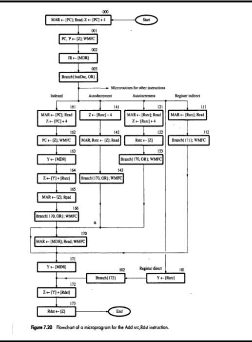
5.10.2BRANCH ADDRESS MODIFICATION USING BIT-ORING
The branch address is determined by ORing particular bit or bits with the current address of microinstruction.
Eg: If the current address is 170 and branch address is 171 then the branch address can be generated by ORing 01(bit 1), with the current address.
Consider the point labeled

in the figure. At this point, it is necessary to choose between direct and indirect addressing modes.
If indirect-mode is specified in the instruction, then the microinstruction in location 170 is performed to fetch the operand from the memory.
If direct-mode is specified, this fetch must be bypassed by branching immediately to location 171.
The most efficient way to bypass microinstruction 170 is to have bit-ORing of
current address 170 &
branch address 171.
5.10.2.1 WIDE BRANCH ADDRESSING
The instruction-decoder (InstDec) generates the starting-address of the microroutine that implements the instruction that has just been loaded into the IR.
Here, register IR contains the Add instruction, for which the instruction decoder generates the microinstruction address 101. (However, this address cannot be loaded as is into the μPC).
The source-operand can be specified in any of several addressing-modes. The bit-ORing technique can be used to modify the starting-address generated by the instruction-decoder to reach the appropriate path.
Use of WMFC
WMFC signal is issued at location 112 which causes a branch to the microinstruction in location 171.
WMFC signal means that the microinstruction may take several clock cycles to complete. If the branch is allowed to happen in the first clock cycle, the microinstruction at location 171 would be
fetched and executed prematurely. To avoid this problem, WMFC signal must inhibit any change in the contents of the μPC during the waiting-period.
Detailed Examination of Add (Rsrc)+,Rdst
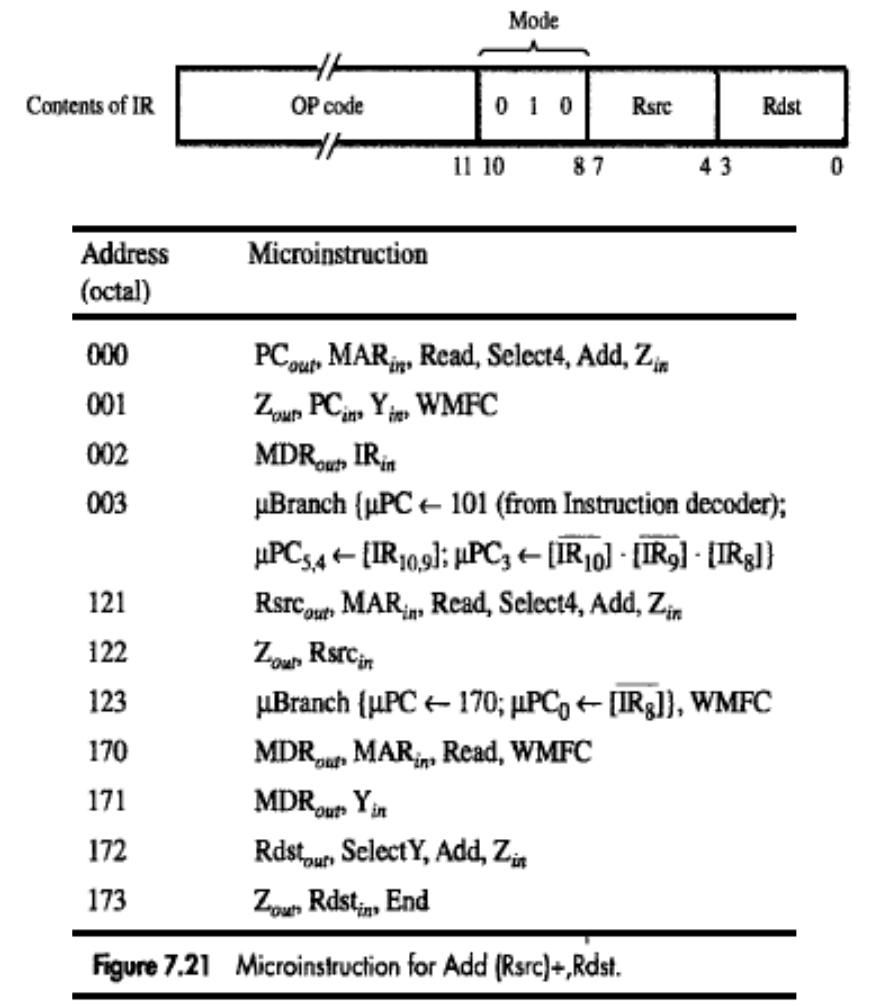
Consider ADD (RSRC)+,RDST; which adds Rsrc content to Rdst content, then stores the sum in Rdst and finally increments Rsrc by 4 (i.e. auto-increment mode).
In bit 10 and 9, bit-patterns 11, 10, 01 and 00 denote indexed, auto-decrement, auto-increment and register modes respectively. For each of these modes, bit 8 is used to specify the indirect version.
The processor has 16 registers that can be used for addressing purposes; each specified using a 4-bit-code (Figure 7.21).
There are 2 stages of decoding:
The microinstruction field must be decoded to determine that an Rsrc or Rdst register is involved.
The decoded output is then used to gate the contents of the Rsrc or Rdst fields in the R into a second decoder, which produces the gating-signals for the actual registers R0 to R15.

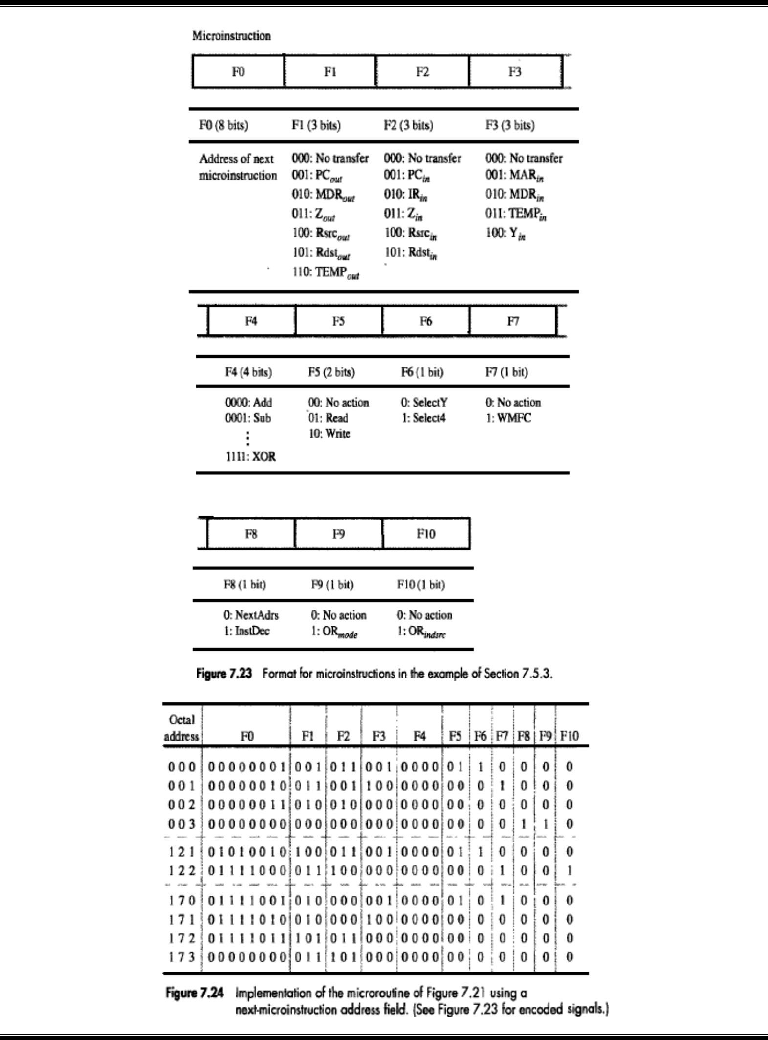
MICROINSTRUCTIONS WITH NEXT-ADDRESS FIELDS
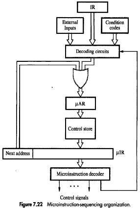
Drawback of previous organization:
The microprogram requires several branch microinstructions which perform no useful
operation. Thus, they detract from the operating-speed of the computer.
Solution:
Include an address-field as a part of every microinstruction to indicate the location of the next microinstruction to be fetched. (Thus, every microinstruction becomes a branch microinstruction).
The flexibility of this approach comes at the expense of additional bits for the address-field(Fig 7.22).
Advantage: Separate branch microinstructions are virtually eliminated. (Figure 7.23-24).
Disadvantage: Additional bits for the address field (around 1/6).
There is no need for a counter to keep track of sequential address. Hence, μPC is replaced with μAR.
The next-address bits are fed through the OR gate to the μAR, so that the address can be modified
on the basis of the data in the IR, external inputs and condition-codes.
The decoding circuits generate the starting-address of a given microroutine on the basis of the opcode in the IR. (μAR Microinstruction Address Register).